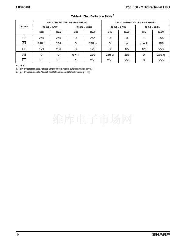
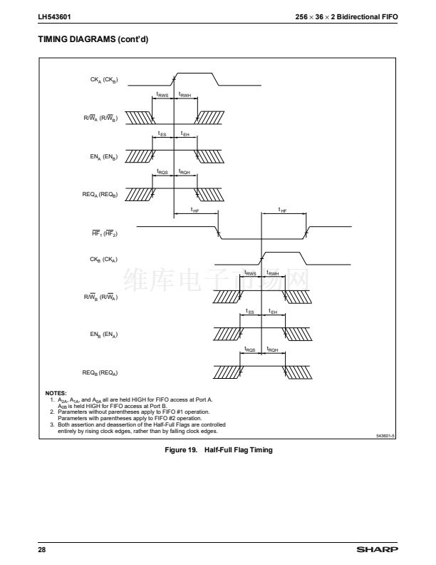
LH543601
256
脳
36
脳
2 Bidirectional FIFO
(CK
A
or CK
B
) whenever: the appropriate enable (EN
A
or
EN
B
) is held HIGH; the appropriate request (REQ
A
or
REQ
B
) is held HIGH; the appropriate Read/Write control
(R/W
A
or R/W
B
) is held LOW; the FIFO address is
selected for the address inputs (A
2A
鈥?A
0A
or A
0B
); and
the prescribed setup times and hold times are observed
for all of these signals. Setup times and hold times must
also be observed on the data-bus pins (D
0A
鈥?D
35A
or
D
0B
鈥?D
35B
).
Normally, the appropriate Output Enable signal (OE
A
or OE
B
) is HIGH, to disable the outputs at that port, so
that the data word present on the bus from external
sources gets stored. However, a 鈥榣oopback鈥?mode of
operation also is possible, in which the data word supplied
by the outputs of one internal FIFO is 鈥榯urned around鈥?at
the port and read back into the other FIFO. In this mode,
the outputs at the port are not disabled. To remain within
specification for all timing parameters, the Clock Cycle
Frequency must be reduced slightly below the value
which otherwise would be permissible for that speed
grade of LH543601.
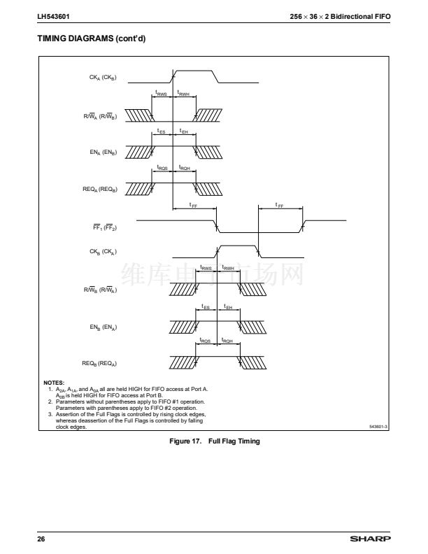
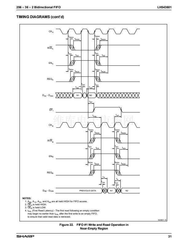
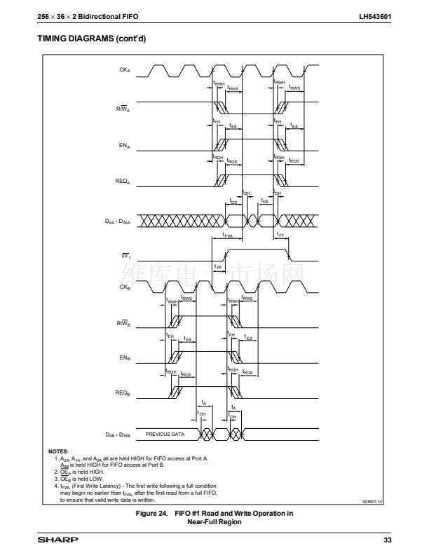
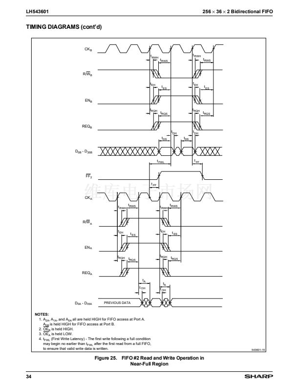
When a FIFO full condition is reached, write operations
are locked out. Following the first read operation from a
full FIFO, another memory location is freed up, and the
corresponding Full Flag is deasserted (FF = HIGH). The
first write operation should begin no earlier than a First
Write Latency (t
FWL
) after the first read operation from a
full FIFO, to ensure that correct read data are retrieved.
FIFO Read
Port A reads from FIFO #2, and Port B reads from FIFO
#1. A read operation is initiated on the rising edge of
a clock (CK
A
or CK
B
) whenever: the appropriate enable
(EN
A
or EN
B
) is held HIGH; the appropriate request
(REQ
A
or REQ
B
) is held HIGH; the appropriate
Read/Write control (R/W
A
or R/W
B
) is held HIGH;
the FIFO address is selected for the address inputs
(A
2A
鈥?A
0A
or A
0B
); and the prescribed setup times and
hold times are observed for all of these signals. Read data
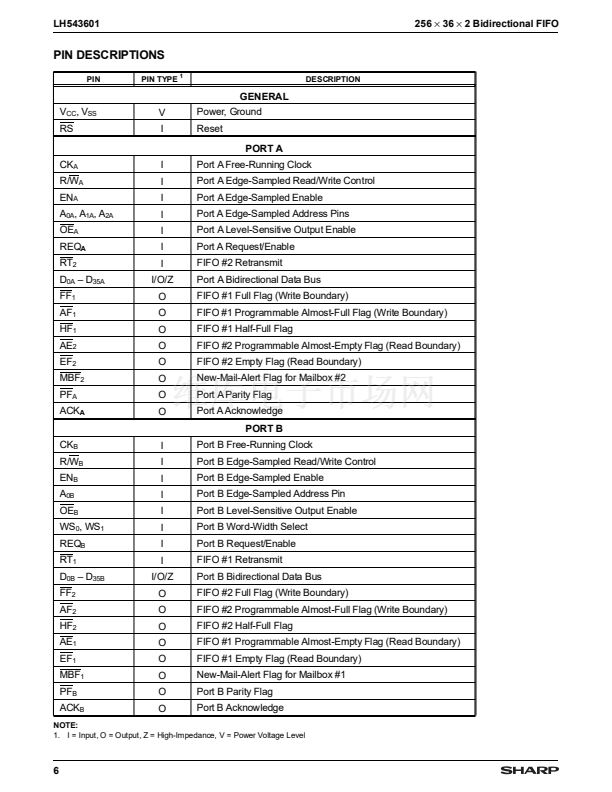
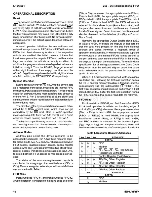
Table 1. Resource-Register Addresses
A
2A
A
1A
A
0A
RESOURCE
PORT A
OPERATIONAL DESCRIPTION
Reset
The device is reset whenever the asynchronous Reset
(RS) input is taken LOW, and at least one rising edge and
one falling edge of both CK
A
and CK
B
occur while RS is
LOW. A reset operation is required after power-up, before
the first write operation may occur. The LH543601 is fully
ready for operation after being reset. No device program-
ming is required if the default states described below are
acceptable.
A reset operation initializes the read-address and
write-address pointers for FIFO #1 and FIFO #2 to those
FIFO鈥檚 first physical memory locations. If the respective
outputs are enabled, the initial contents of these first
locations appear at the outputs. FIFO and mailbox status
flags are updated to indicate an empty condition. In
addition, the programmable-status-flag offset values are
initialized to eight. Thus, the AE
1
/AE
2
flags get asserted
within eight locations of an empty condition, and the
AF
1
/AF
2
flags likewise get asserted within eight locations
of a full condition, for FIFO #1/FIFO #2 respectively.
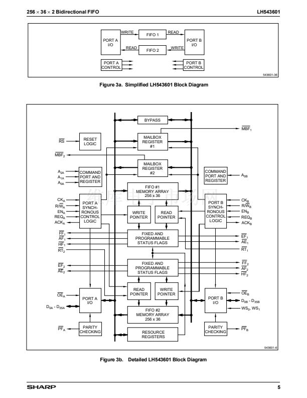
Bypass Operation
During reset (whenever RS is LOW) the device acts
as a registered transceiver, bypassing the internal FIFO
memories. Port A acts as the master port. A write or read
operation on Port A during reset transfers data directly to
or from Port B. Port B is considered to be the slave, and
cannot perform write or read operations independently on
its own during reset.
The direction of the bypass data transmission is deter-
mined by th R/W
A
control input, which does not get
overridden by the RS input. Here, a 鈥榳rite鈥?operation
means passing data from Port A to Port B, and a 鈥榬ead鈥?/div>
operation means passing data from Port B to Port A.
The bypass capability may be used to pass initializa-
tion or configuration data directly between a master proc-
essor and a peripheral device during reset.
Address Modes
Address pins select the device resource to be
accessed by each port. Port A has three resource-regis-
ter-select inputs, A
0A
, A
1A
, and A
2A
, which select between
FIFO access, mailbox-register access, control-register
access (write only), and programmable flag-offset-value-
register access. Port B has a single address input, A
0B
,
to select between FIFO access or mailbox-register ac-
cess.
The status of the resource-register-select inputs is
sampled at the rising edge of an enabled clock (CK
A
or
CK
B
). Resource-register select-input address definitions
are summarized in Table 1.
FIFO Write
Port A writes to FIFO #1, and Port B writes to FIFO #2.
A write operation is initiated on the rising edge of a clock
H
H
H
H
L
L
L
L
H
H
L
L
H
H
L
L
A
0B
H
L
H
L
H
L
H
L
FIFO
Mailbox
AF
2
, AE
2
, AF
1
, AE
1
Flag Offsets
Register (36-Bit Mode)
Control Register (Parity Mode)
AE
1
Flag Offset Register
AF
1
Flag Offset Register
AE
2
Flag Offset Register
AF
2
Flag Offset Register
RESOURCE
PORT B
H
L
FIFO
Mailbox
10


 1
1
 2
2
 3
3
 4
4
 5
5
 6
6
 7
7
 8
8
 9
9
 10
10
 11
11
 12
12
 13
13
 14
14
 15
15
 16
16
 17
17
 18
18
 19
19
 20
20
 21
21
 22
22
 23
23
 24
24
 25
25
 26
26
 27
27
 28
28
 29
29
 30
30
 31
31
 32
32
 33
33
 34
34
 35
35
 36
36
 37
37
 38
38
 39
39
 40
40
 41
41
 42
42
 43
43
