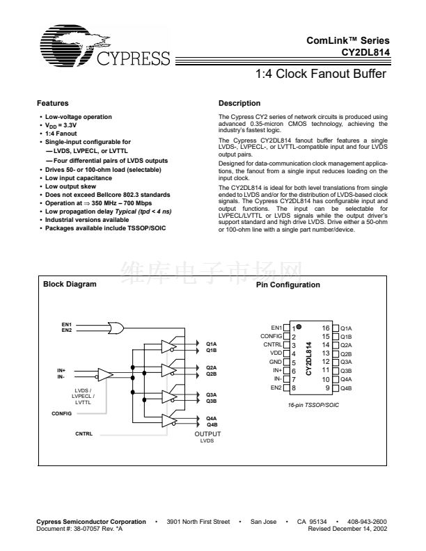
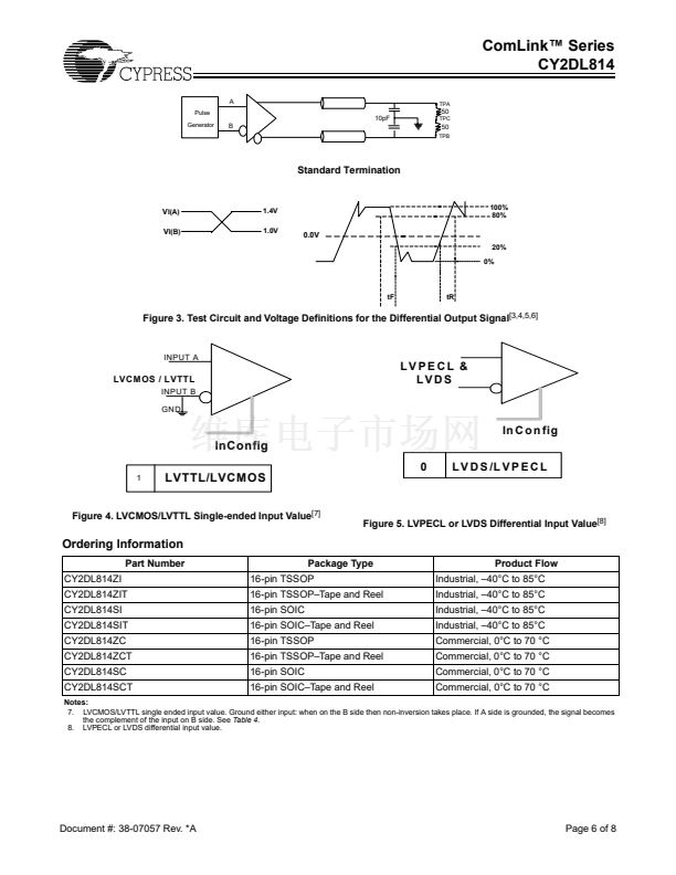
Differential input pair or single line.
LVPECL default. See config below.
Converts into a High drive driver from a standard LVDS.
鈥?/div>
), (EN, EN#) from the default
LVPECL/LVDS (logic = 0)
To LVTTL/LVCMOS (logic = 1)
Enable/disable logic. See
Table 1
below for details.
Differential outputs.
2
CONFIG
LVTTL/LVCMOS
1,8
16,15,14,13
12,11,10,9
EN1, EN2
Q1A, Q1B, Q2A,
Q2B,
Q3A, Q3B, Q4A,
Q4B
V
DD
LVTTL/LVCMOS
LDVS
4
5
POWER
POWER
Positive supply voltage
Ground
G
ND
Maximum Ratings
[1][2]
Storage Temperature: ................................鈥?5掳C to + 150掳C
Ambient Temperature:................................... 鈥?0掳C to +85掳C
Supply Voltage to Ground Potential
(Inputs and V
CC
only)....................................... 鈥?.3V to 4.6V
Supply Voltage to Ground Potential
Table 1. EN1 EN2 Function Table鈥揇ifferential Input Mode
Enable Logic
EN1
H
H
X
X
L
EN2
X
X
L
L
H
IN+
H
L
H
L
X
Input
IN鈥?/div>
L
H
L
H
X
QnA
H
L
H
L
Z
Outputs
QnB
L
H
L
H
Z
(Outputs only) ........................................ 鈥?.3V to V
DD
+ 0.3V
DC Input Voltage ................................... 鈥?.3V to V
DD
+ 0.3V
DC Output Voltage................................. 鈥?.3V to V
DD
+ 0.9V
Power Dissipation........................................................ 0.75W
Table 2. Output Drive Control for Standard and Bus/B/High Drive B
CNTRL Pin 3 Binary Value
0
1
Drive STD
Standard
High Drive/Bus/B
Impedance
100 ohm
50 ohm
100 ohm
50 ohm
Output Voltage Value
V0 = Voutput
V = 1/2 * V0
V = 2 * V0
V = V0
Note:
1. Stresses greater than those listed under absolute maximum ratings may cause permanent damage to the device. This is intended to be a stress rating only and
functional operation of the device at these or any other conditions above those indicated in the operation sections of this specification is not implied. Exposure
to absolute maximum rating conditions for extended periods may affect reliability.
2. Multiple Supplies: The voltage on any input or I/O pin cannot exceed the power pin during power-up. Power supply sequencing is NOT required.
Document #: 38-07057 Rev. *A
Page 2 of 8


 1
1
 2
2
 3
3
 4
4
 5
5
 6
6
 7
7
 8
8
