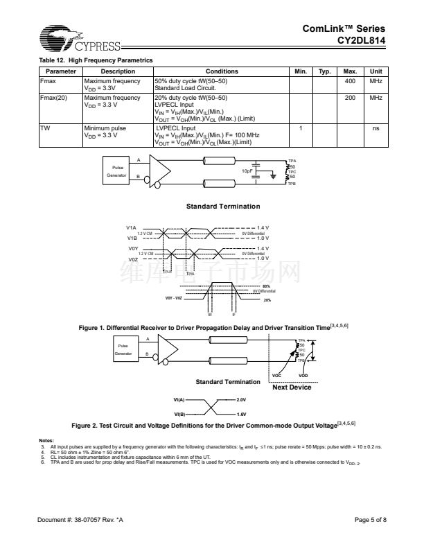
defaulting to 100 ohm output drivers. RL and CL to G
Pin control (pin 3) logic is 鈥淭rue鈥?/div>
defaulting to 50 ohm output drivers.
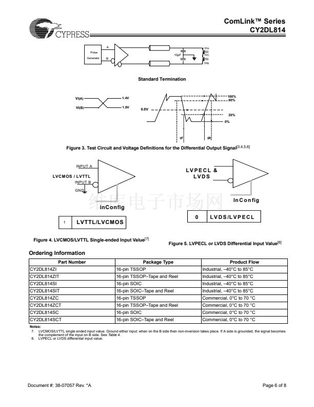
Differential 20% to 80%
CL鈥?0 pF
RL and CL to G
ND
3 CL = C
intrinsic
and C
external
Fall Time
Rise Time
RL = 50 ohm
Output boost
350
1.4
600
ns
ps
Fall Time
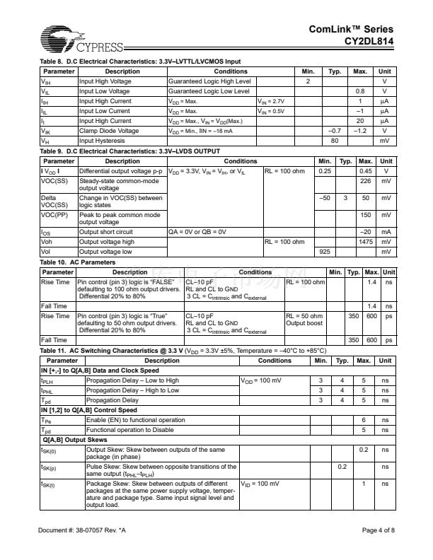
Table 11. AC Switching Characteristics @ 3.3 V
(V
DD
= 3.3V 卤5%, Temperature = 鈥?0掳C to +85掳C)
Parameter
t
PLH
t
PHL
T
pd
T
Pe
T
pd
t
SK(0)
t
SK(p)
t
SK(t)
Description
Propagation Delay 鈥?Low to High
Propagation Delay 鈥?High to Low
Propagation Delay
Enable (EN) to functional operation
Functional operation to Disable
Output Skew: Skew between outputs of the same
package (in phase)
Pulse Skew: Skew between opposite transitions of the
same output (t
PHL
鈥搕
PLH
)
Package Skew: Skew between outputs of different
V
ID
= 100 mV
packages at the same power supply voltage, temper-
ature and package type. Same input signal level and
output load.
0.2
Conditions
V
OD
= 100 mV
Min.
3
3
3
350
Typ.
4
4
4
600
ps
Unit
ns
ns
ns
ns
ns
ns
ns
Max.
5
5
5
6
5
0.2
IN [+,-] to Q[A,B] Data and Clock Speed
IN [1,2] to Q[A,B] Control Speed
Q[A,B] Output Skews
1
ns
Document #: 38-07057 Rev. *A
Page 4 of 8


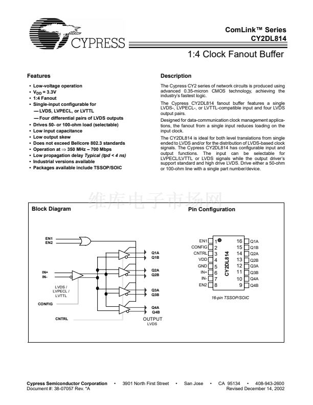 1
1
 2
2
 3
3
 4
4
 5
5
 6
6
 7
7
 8
8
