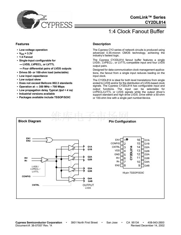
ComLink鈩?Series
CY2DL814
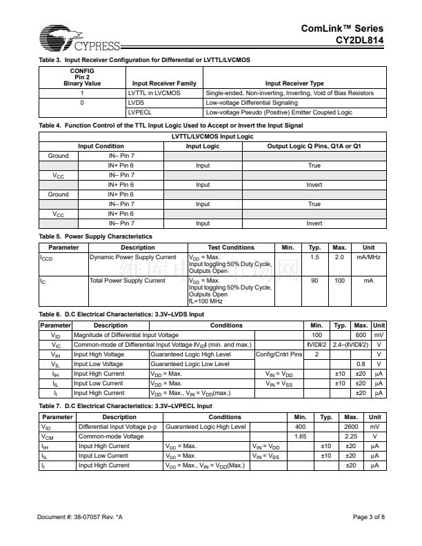
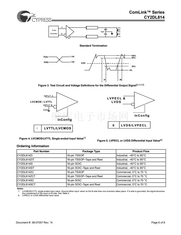
Table 3. Input Receiver Configuration for Differential or LVTTL/LVCMOS
CONFIG
Pin 2
Binary Value
1
0
Input Receiver Family
LVTTL in LVCMOS
LVDS
LVPECL
Input Receiver Type
Single-ended, Non-inverting, Inverting, Void of Bias Resistors
Low-voltage Differential Signaling
Low-voltage Pseudo (Positive) Emitter Coupled Logic
Table 4. Function Control of the TTL Input Logic Used to Accept or Invert the Input Signal
LVTTL/LVCMOS Input Logic
Input Condition
Ground
V
CC
Ground
V
CC
IN鈥?Pin 7
IN+ Pin 6
IN鈥?Pin 7
IN+ Pin 6
IN+ Pin 6
IN鈥?Pin 7
IN+ Pin 6
IN鈥?Pin 7
Table 5. Power Supply Characteristics
Parameter
I
CCD
Description
Dynamic Power Supply Current
Test Conditions
V
DD
= Max.
Input toggling 50% Duty Cycle,
Outputs Open
V
DD
= Max.
Input toggling 50% Duty Cycle,
Outputs Open
fL=100 MHz
Min.
Typ.
1.5
Max.
2.0
Unit
mA/MHz
Input
Invert
Input
True
Input
Invert
Input
True
Input Logic
Output Logic Q Pins, Q1A or Q1
I
C
Total Power Supply Current
90
100
mA
Table 6. D.C Electrical Characteristics: 3.3V鈥揕VDS Input
Parameter
V
ID
V
IC
V
IH
V
IL
I
IH
I
IL
I
I
Description
Magnitude of Differential Input Voltage
Common-mode of Differential Input Voltage
IV
ID
I
(min. and max.)
Input High Voltage
Input Low Voltage
Input High Current
Input Low Current
Input High Current
Guaranteed Logic High Level
Guaranteed Logic Low Level
V
DD
= Max.
V
DD
= Max.
V
DD
= Max., V
IN
= V
DD
(max.)
V
IN
= V
DD
V
IN
= V
SS
卤10
卤10
Config/Cntrl Pins
Conditions
Min.
100
IVIDI/2
2
0.8
卤20
卤20
卤20
Typ.
Max. Unit
600
2.4鈥?IVIDI/2)
mV
V
V
V
碌A
碌A
碌A
Table 7. D.C Electrical Characteristics: 3.3V鈥揕VPECL Input
Parameter
V
ID
V
CM
I
IH
I
IL
I
I
Description
Differential Input Voltage p-p
Common-mode Voltage
Input High Current
Input Low Current
Input High Current
V
DD
= Max.
V
DD
= Max.
V
DD
= Max., V
IN
= V
DD
(Max.)
V
IN
= V
DD
V
IN
= V
SS
Conditions
Guaranteed Logic High Level
Min.
400
1.65
卤10
卤10
Typ.
Max.
2600
2.25
卤20
卤20
卤20
Unit
mV
V
碌A
碌A
碌A
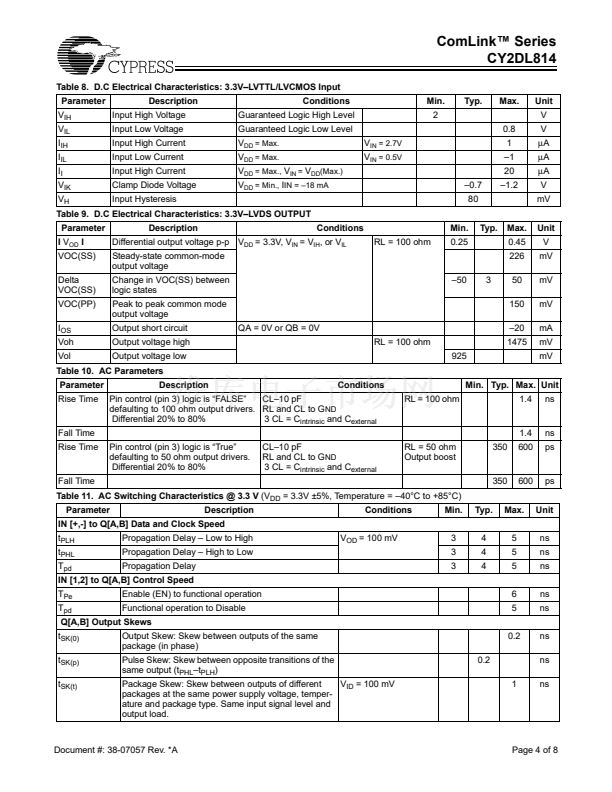
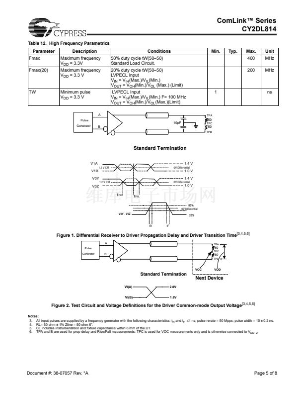
Document #: 38-07057 Rev. *A
Page 3 of 8


 1
1
 2
2
 3
3
 4
4
 5
5
 6
6
 7
7
 8
8
