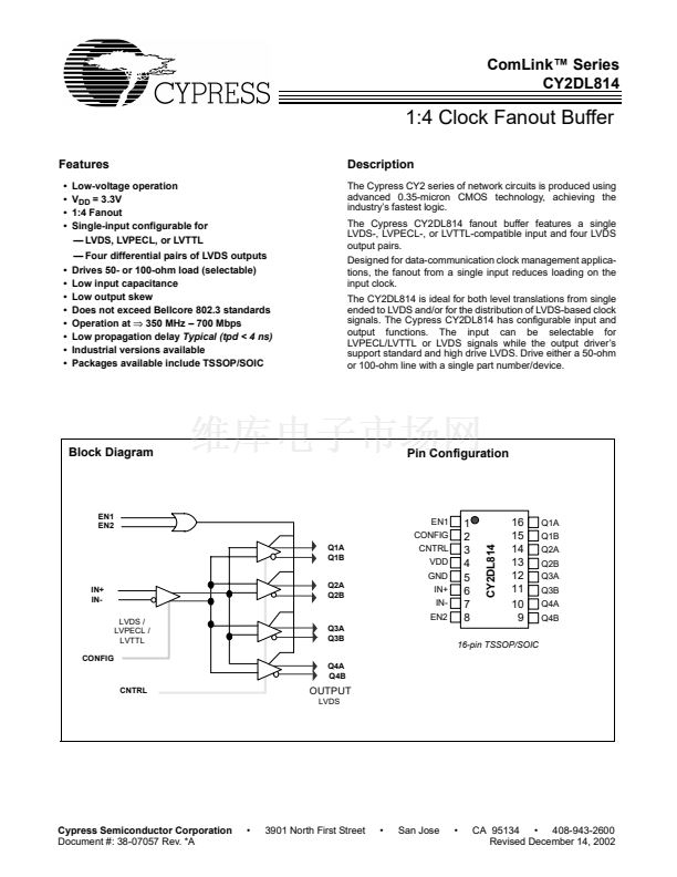
ComLink鈩?Series
CY2DL814
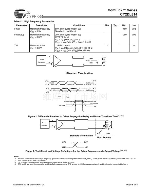
Table 12. High Frequency Parametrics
Parameter
Fmax
Fmax(20)
Description
Maximum frequency
V
DD
= 3.3V
Maximum frequency
V
DD
= 3.3 V
Conditions
50% duty cycle tW(50鈥?0)
Standard Load Circuit.
20% duty cycle tW(50鈥?0)
LVPECL Input
V
IN
= V
IH
(Max.)/V
IL
(Min.)
V
OUT
= V
OH
(Min.)/V
OL
(Max.) (Limit)
LVPECL Input
V
IN
= V
IH
(Max.)/V
IL
(Min.) F= 100 MHz
V
OUT
= V
OH
(Min.)/V
OL
(Max.)(Limit)
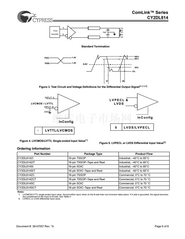
A
Pulse
Generator
TPA
Min.
Typ.
Max.
400
200
Unit
MHz
MHz
TW
Minimum pulse
V
DD
= 3.3 V
1
ns
10pF
B
50
TPC
50
TPB
Standard Termination
V1A
1.2 V CM
1.4 V
0V Differential
V1B
V0Y
1.2 V CM
1.0 V
1.4 V
0V Differential
V0Z
T
PLH
T
PHL
1.0 V
80%
0V Differential
V0Y - V0Z
20%
tR
tF
Figure 1. Differential Receiver to Driver Propagation Delay and Driver Transition Time
[3,4,5,6]
A
Pulse
Generator
TPA
50
TPC
B
50
TPB
VOC
VOD
Standard Termination
V
I(A)
V
I(B)
2.0V
1.6V
Next Device
Figure 2. Test Circuit and Voltage Definitions for the Driver Common-mode Output Voltage
[3,4,5,6]
Notes:
3. All input pulses are supplied by a frequency generator with the following characteristics: t
R
and t
F
鈮?/div>
1 ns; pulse rerate = 50 Mpps; pulse width = 10 卤 0.2 ns.
4. RL= 50 ohm 卤 1% Zline = 50 ohm 6鈥?
5. CL includes instrumentation and fixture capacitance within 6 mm of the UT.
6. TPA and B are used for prop delay and Rise/Fall measurements. TPC is used for VOC measurements only and is otherwise connected to V
DD- 2
.
Document #: 38-07057 Rev. *A
Page 5 of 8


 1
1
 2
2
 3
3
 4
4
 5
5
 6
6
 7
7
 8
8
