ComLink鈩?Series
CY2DL814
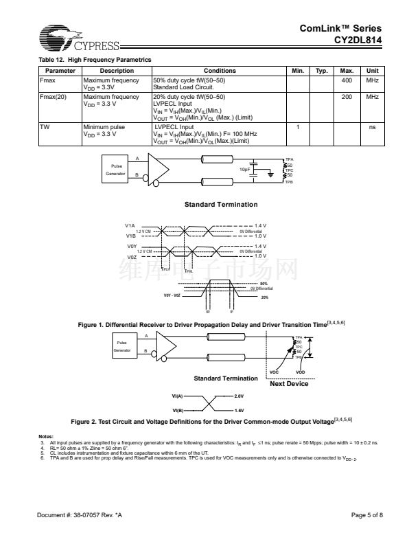
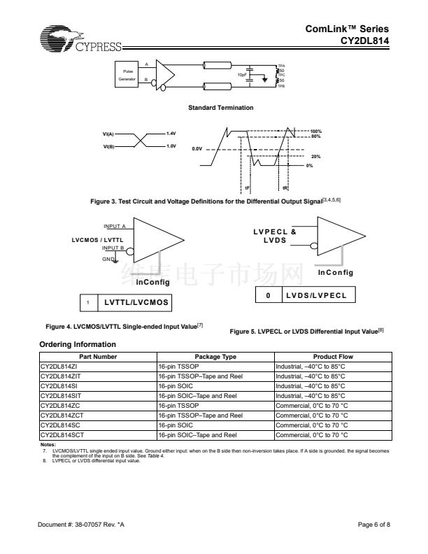
A
Pulse
Generator
TPA
10pF
B
50
TPC
50
TPB
Standard Termination
V
I(A)
V
I(B)
1.4V
1.0V
100%
80%
0.0V
20%
0%
tF
tR
Figure 3. Test Circuit and Voltage Definitions for the Differential Output Signal
[3,4,5,6]
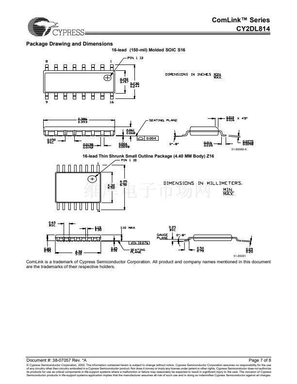
INPUT A
LVCM OS / LVTTL
INPUT B
GND
LVPECL &
LVDS
In C o n fig
InConfig
0
1
L V D S /L V P E C L
LVTTL/LVCMOS
Figure 4. LVCMOS/LVTTL Single-ended Input Value
[7]
Figure 5. LVPECL or LVDS Differential Input Value
[8]
Ordering Information
Part Number
CY2DL814ZI
CY2DL814ZIT
CY2DL814SI
CY2DL814SIT
CY2DL814ZC
CY2DL814ZCT
CY2DL814SC
CY2DL814SCT
Package Type
16-pin TSSOP
16-pin TSSOP鈥揟ape and Reel
16-pin SOIC
16-pin SOIC鈥揟ape and Reel
16-pin TSSOP
16-pin TSSOP鈥揟ape and Reel
16-pin SOIC
16-pin SOIC鈥揟ape and Reel
Product Flow
Industrial, 鈥?0掳C to 85掳C
Industrial, 鈥?0掳C to 85掳C
Industrial, 鈥?0掳C to 85掳C
Industrial, 鈥?0掳C to 85掳C
Commercial, 0掳C to 70 掳C
Commercial, 0掳C to 70 掳C
Commercial, 0掳C to 70 掳C
Commercial, 0掳C to 70 掳C
Notes:
7. LVCMOS/LVTTL single ended input value. Ground either input: when on the B side then non-inversion takes place. If A side is grounded, the signal becomes
the complement of the input on B side. See
Table 4.
8. LVPECL or LVDS differential input value.
Document #: 38-07057 Rev. *A
Page 6 of 8


 1
1
 2
2
 3
3
 4
4
 5
5
 6
6
 7
7
 8
8
