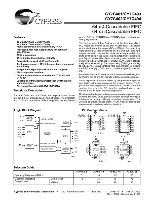
CY7C401/CY7C403
CY7C402/CY7C404
Maximum Ratings
(Above which the useful life may be impaired. For user guide-
lines, not tested.)
Storage Temperature ................................. 鈥?5掳C to +150掳C
Ambient Temperature with
Power Applied............................................. 鈥?5掳C to +125掳C
Supply Voltage to Ground Potential ............... 鈥?.5V to +7.0V
DC Voltage Applied to Outputs
in High Z State ............................................... 鈥?.5V to +7.0V
DC Input Voltage............................................ 鈥?.0V to +7.0V
Power Dissipation ..........................................................1.0W
Output Current, into Outputs (LOW)............................ 20 mA
Static Discharge Voltage ........................................... >2001V
(per MIL-STD-883, Method 3015)
Latch-Up Current ..................................................... >200 mA
Operating Range
Range
Commercial
Military
[1]
Ambient
Temperature
0
掳
C to +70
掳
C
鈥?5
掳
C to +125
掳
C
V
CC
5V
卤10%
5V
卤10%
Electrical Characteristics
Over the Operating Range (Unless Otherwise Noted)
[2]
7C40X鈥?0, 15, 25
Parameter
V
OH
V
OL
V
IH
V
IL
I
IX
V
CD[3]
I
OZ
I
OS
I
CC
Description
Output HIGH Voltage
Output LOW Voltage
Input HIGH Voltage
Input LOW Voltage
Input Leakage Current
Input Diode Clamp Voltage
[3]
Output Leakage Current
Output Short Circuit Current
[4]
Power Supply Current
GND
鈮?/div>
V
OUT
鈮?/div>
V
CC
, V
CC
= 5.5V
Output Disabled (CY7C403 and CY7C404)
V
CC
= Max., V
OUT
= GND
V
CC
= Max., I
OUT
= 0 mA
Commercial
Military
鈥?0
+50
鈥?0
75
90
碌A
mA
mA
mA
GND
鈮?/div>
V
I
鈮?/div>
V
CC
Test Conditions
V
CC
= Min., I
OH
= 鈥?.0 mA
V
CC
= Min., I
OL
= 8.0 mA
2.0
鈥?.0
鈥?0
Min.
2.4
0.4
6.0
0.8
+10
Max.
Unit
V
V
V
V
碌A
Capacitance
[5]
Parameter
C
IN
C
OUT
Description
Input Capacitance
Output Capacitance
Test Conditions
T
A
= 25掳C, f = 1 MHz,
V
CC
= 4.5V
Max.
5
7
Unit
pF
pF
Notes:
1. T
A
is the 鈥渋nstant on鈥?case temperature.
2. See the last page of this specification for Group A subgroup testing information.
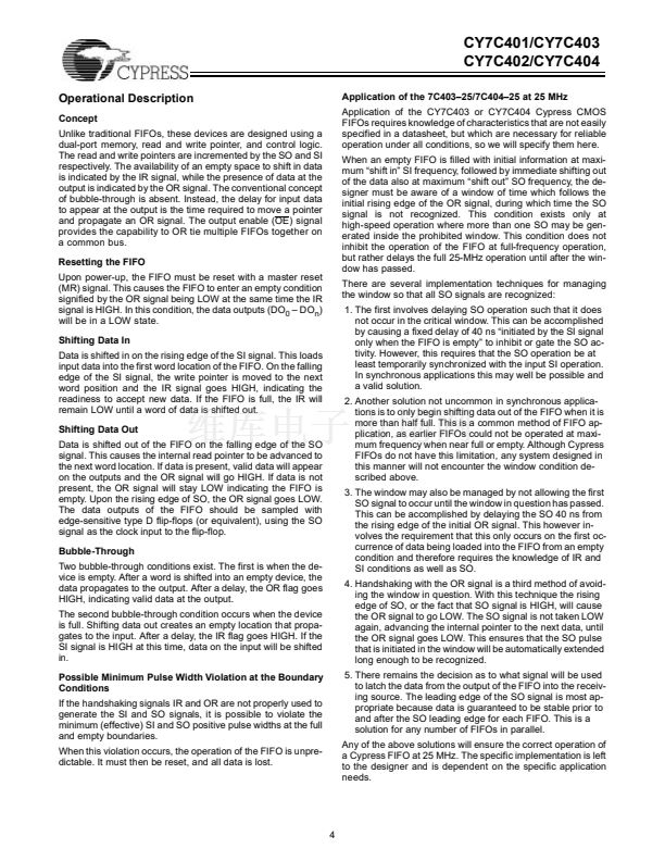
3. The CMOS process does not provide a clamp diode. However, the FIFO is insensitive to 鈥?V dc input levels and 鈥?V undershoot pulses of less than 10 ns
(measured at 50% output).
4. For test purposes, not more than one output at a time should be shorted. Short circuit test duration should not exceed 30 seconds.
5. Tested initially and after any design or process changes that may affect these parameters.
2


 1
1
 2
2
 3
3
 4
4
 5
5
 6
6
 7
7
 8
8
 9
9
 10
10
 11
11
 12
12
 13
13
