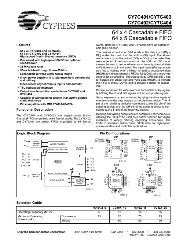
鈥?/div>
0
5
10
5
30
20
20
30
35
40
40
40
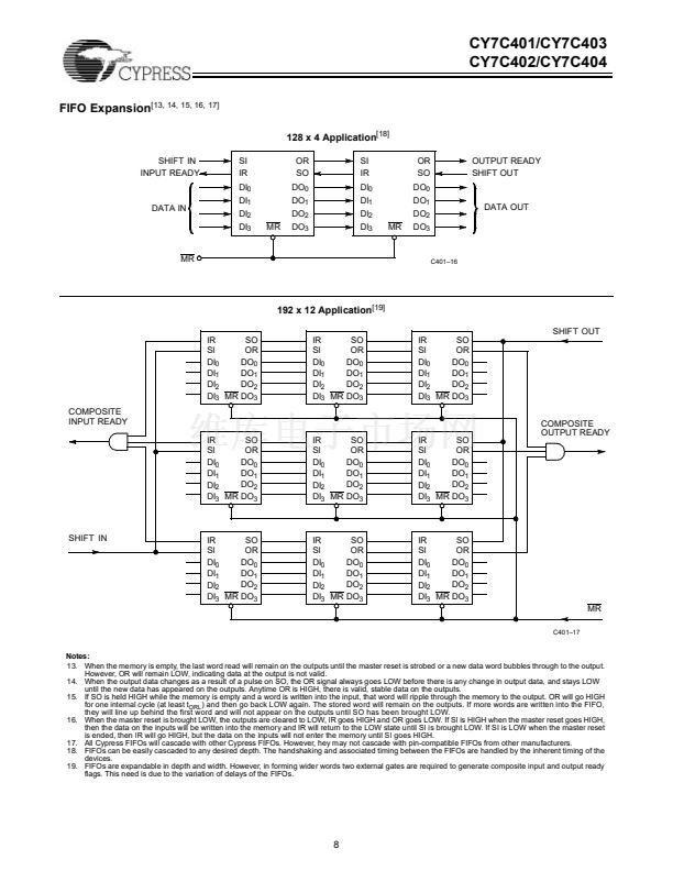
35
30
95
20
25
40
55
0
5
10
5
30
20
20
25
25
35
35
35
30
25
65
7C401鈥?
7C402鈥?
Min.
Max.
5
20
30
0
40
40
45
20
25
35
40
0
5
10
5
20
15
15
25
10
35
35
25
20
15
50/60
7C40X鈥?0
Min.
Max.
10
20
25
0
30
35
40
11
20
19/21
34/37
7C40X鈥?5
Min.
Max.
15
11
20
0
20
21/22
28/30
7C40X鈥?5
[7]
Min.
Max.
25
Unit
MHz
ns
ns
ns
ns
ns
ns
ns
ns
ns
ns
ns
ns
ns
ns
ns
ns
ns
ns
ns
ns
ns
ns
ns
ns
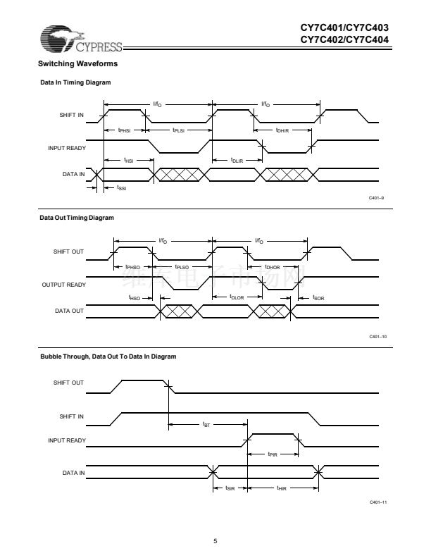
Parameter
f
O
t
PHSI
t
PLSI
t
SSI
t
HSI
t
DLIR
t
DHIR
t
PHSO
t
PLSO
t
DLOR
t
DHOR
t
SOR
t
HSO
t
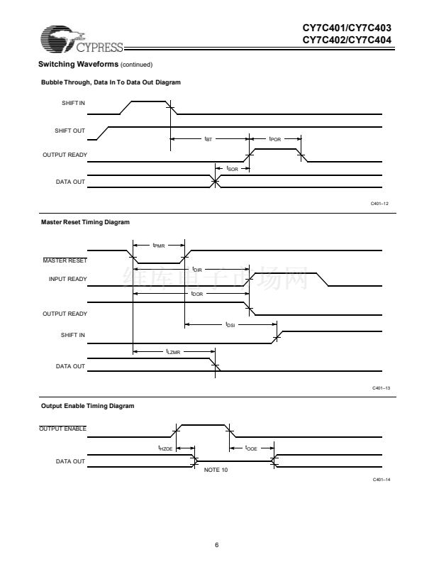
BT
t
SIR
t
HIR
t
PIR
t
POR
t
PMR
t
DSI
t
DOR
t
DIR
t
LZMR
t
OOE
t
HZOE
Description
Operating Frequency
SI HIGH Time
SO LOW Time
Data Set-Up to SI
Data Hold from SI
Delay, SI HIGH to IR LOW
Delay, SI LOW to IR HIGH
SO HIGH Time
SO LOW Time
Delay, SO HIGH to OR LOW
Delay, SO LOW to OR HIGH
Data Set-Up to OR HIGH
Data Hold from SO LOW
Bubble-Through Time
Data Set-Up to IR
Data Hold from IR
Input Ready Pulse HIGH
Output Ready Pulse HIGH
MR Pulse Width
MR HIGH to SI HIGH
MR LOW to OR LOW
MR LOW to IR HIGH
MR LOW to Output LOW
Output Valid from OE LOW
Output High Z from OE HIGH
Notes:
6. Test conditions assume signal transition time of 5 ns or less, timing reference levels of 1.5V and output loading of the specified I
OL
/I
OH
and 30-pF load
capacitance, as in part (a) of AC Test Loads and Waveforms.
7. Commercial/Military
8. I/f
O
> t
PHSI
+ t
DHIR
, I/f
O
> t
PHSO
+ t
DHOR
9. t
SSI
and t
HSI
apply when memory is not full.
10. t
SIR
and t
HIR
apply when memory is full, SI is high and minimum bubble-through (t
BT
) conditions exist.
11. All data outputs will be at LOW level after reset goes HIGH until data is entered into the FIFO.
12. HIGH-Z transitions are referenced to the steady-state V
OH
鈥?00 mV and V
OL
+500 mV levels on the output. t
HZOE
is tested with 5-pF load capacitance as
in part (b) of AC Test Loads and Waveforms.
3


 1
1
 2
2
 3
3
 4
4
 5
5
 6
6
 7
7
 8
8
 9
9
 10
10
 11
11
 12
12
 13
13
