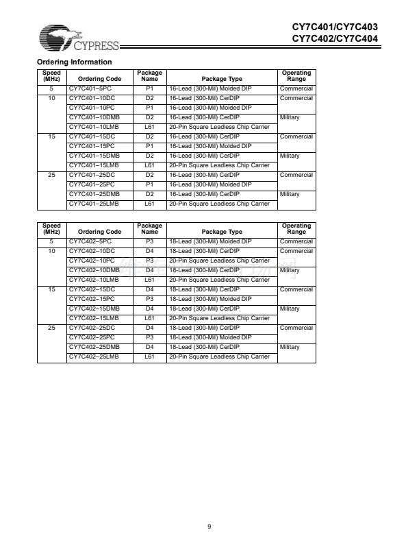
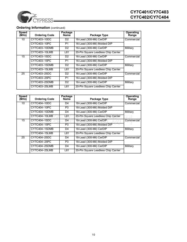
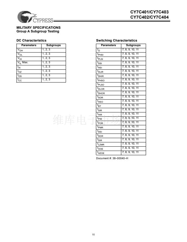
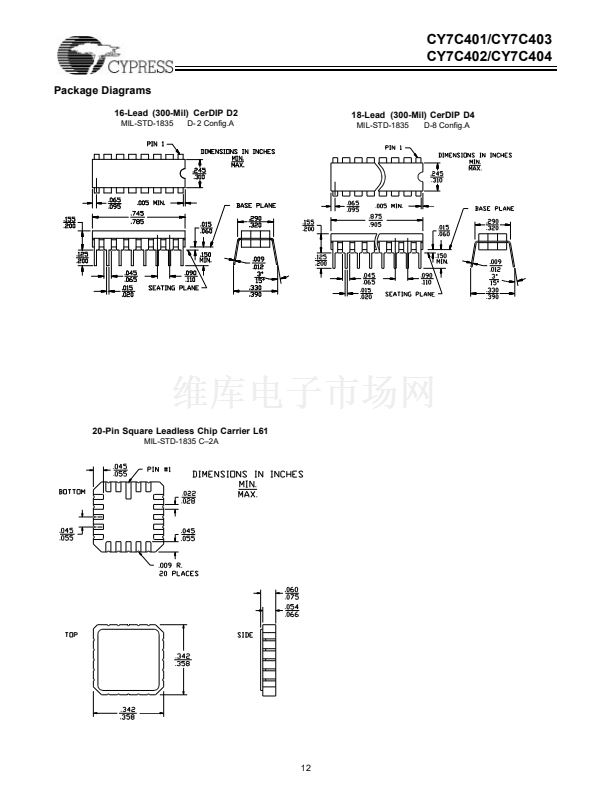
CY7C401/CY7C403
CY7C402/CY7C404
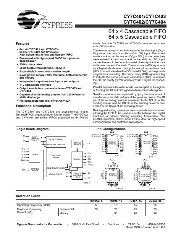
Operational Description
Concept
Unlike traditional FIFOs, these devices are designed using a
dual-port memory, read and write pointer, and control logic.
The read and write pointers are incremented by the SO and SI
respectively. The availability of an empty space to shift in data
is indicated by the IR signal, while the presence of data at the
output is indicated by the OR signal. The conventional concept
of bubble-through is absent. Instead, the delay for input data
to appear at the output is the time required to move a pointer
and propagate an OR signal. The output enable (OE) signal
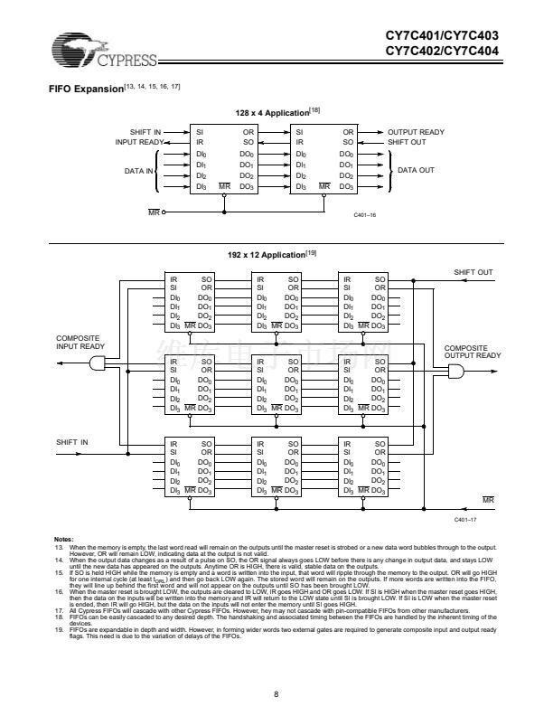
provides the capability to OR tie multiple FIFOs together on
a common bus.
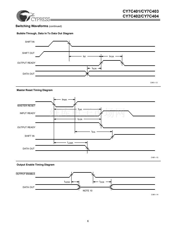
Resetting the FIFO
Upon power-up, the FIFO must be reset with a master reset
(MR) signal. This causes the FIFO to enter an empty condition
signified by the OR signal being LOW at the same time the IR
signal is HIGH. In this condition, the data outputs (DO
0
鈥?DO
n
)
will be in a LOW state.
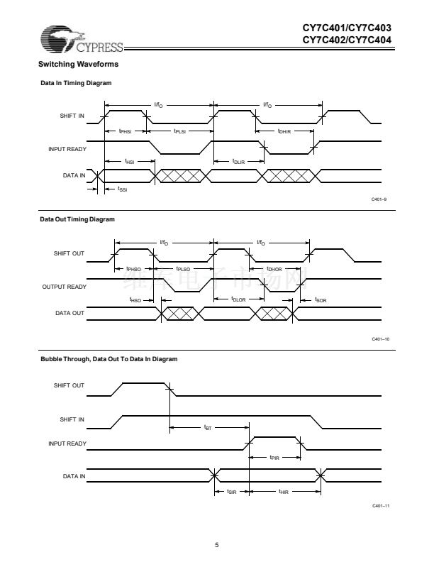
Shifting Data In
Data is shifted in on the rising edge of the SI signal. This loads
input data into the first word location of the FIFO. On the falling
edge of the SI signal, the write pointer is moved to the next
word position and the IR signal goes HIGH, indicating the
readiness to accept new data. If the FIFO is full, the IR will
remain LOW until a word of data is shifted out.
Shifting Data Out
Data is shifted out of the FIFO on the falling edge of the SO
signal. This causes the internal read pointer to be advanced to
the next word location. If data is present, valid data will appear
on the outputs and the OR signal will go HIGH. If data is not
present, the OR signal will stay LOW indicating the FIFO is
empty. Upon the rising edge of SO, the OR signal goes LOW.
The data outputs of the FIFO should be sampled with
edge-sensitive type D flip-flops (or equivalent), using the SO
signal as the clock input to the flip-flop.
Bubble-Through
Two bubble-through conditions exist. The first is when the de-
vice is empty. After a word is shifted into an empty device, the
data propagates to the output. After a delay, the OR flag goes
HIGH, indicating valid data at the output.
The second bubble-through condition occurs when the device
is full. Shifting data out creates an empty location that propa-
gates to the input. After a delay, the IR flag goes HIGH. If the
SI signal is HIGH at this time, data on the input will be shifted
in.
Possible Minimum Pulse Width Violation at the Boundary
Conditions
If the handshaking signals IR and OR are not properly used to
generate the SI and SO signals, it is possible to violate the
minimum (effective) SI and SO positive pulse widths at the full
and empty boundaries.
When this violation occurs, the operation of the FIFO is unpre-
dictable. It must then be reset, and all data is lost.
Application of the 7C403鈥?5/7C404鈥?5 at 25 MHz
Application of the CY7C403 or CY7C404 Cypress CMOS
FIFOs requires knowledge of characteristics that are not easily
specified in a datasheet, but which are necessary for reliable
operation under all conditions, so we will specify them here.
When an empty FIFO is filled with initial information at maxi-
mum 鈥渟hift in鈥?SI frequency, followed by immediate shifting out
of the data also at maximum 鈥渟hift out鈥?SO frequency, the de-
signer must be aware of a window of time which follows the
initial rising edge of the OR signal, during which time the SO
signal is not recognized. This condition exists only at
high-speed operation where more than one SO may be gen-
erated inside the prohibited window. This condition does not
inhibit the operation of the FIFO at full-frequency operation,
but rather delays the full 25-MHz operation until after the win-
dow has passed.
There are several implementation techniques for managing
the window so that all SO signals are recognized:
1. The first involves delaying SO operation such that it does
not occur in the critical window. This can be accomplished
by causing a fixed delay of 40 ns 鈥渋nitiated by the SI signal
only when the FIFO is empty鈥?to inhibit or gate the SO ac-
tivity. However, this requires that the SO operation be at
least temporarily synchronized with the input SI operation.
In synchronous applications this may well be possible and
a valid solution.
2. Another solution not uncommon in synchronous applica-
tions is to only begin shifting data out of the FIFO when it is
more than half full. This is a common method of FIFO ap-
plication, as earlier FIFOs could not be operated at maxi-
mum frequency when near full or empty. Although Cypress
FIFOs do not have this limitation, any system designed in
this manner will not encounter the window condition de-
scribed above.
3. The window may also be managed by not allowing the first
SO signal to occur until the window in question has passed.
This can be accomplished by delaying the SO 40 ns from
the rising edge of the initial OR signal. This however in-
volves the requirement that this only occurs on the first oc-
currence of data being loaded into the FIFO from an empty
condition and therefore requires the knowledge of IR and
SI conditions as well as SO.
4. Handshaking with the OR signal is a third method of avoid-
ing the window in question. With this technique the rising
edge of SO, or the fact that SO signal is HIGH, will cause
the OR signal to go LOW. The SO signal is not taken LOW
again, advancing the internal pointer to the next data, until
the OR signal goes LOW. This ensures that the SO pulse
that is initiated in the window will be automatically extended
long enough to be recognized.
5. There remains the decision as to what signal will be used
to latch the data from the output of the FIFO into the receiv-
ing source. The leading edge of the SO signal is most ap-
propriate because data is guaranteed to be stable prior to
and after the SO leading edge for each FIFO. This is a
solution for any number of FIFOs in parallel.
Any of the above solutions will ensure the correct operation of
a Cypress FIFO at 25 MHz. The specific implementation is left
to the designer and is dependent on the specific application
needs.
4


 1
1
 2
2
 3
3
 4
4
 5
5
 6
6
 7
7
 8
8
 9
9
 10
10
 11
11
 12
12
 13
13
