= 6鈩?/div>
Gate to source cutoff voltage V
GS(off)
Static drain to source on state R
DS(on)
resistance
Forward transfer admittance
Input capacitance
Output capacitance
|y
fs
|
Ciss
Coss
Reverse transfer capacitance Crss
Total gate charge
Gate to source charge
Gate to drain charge
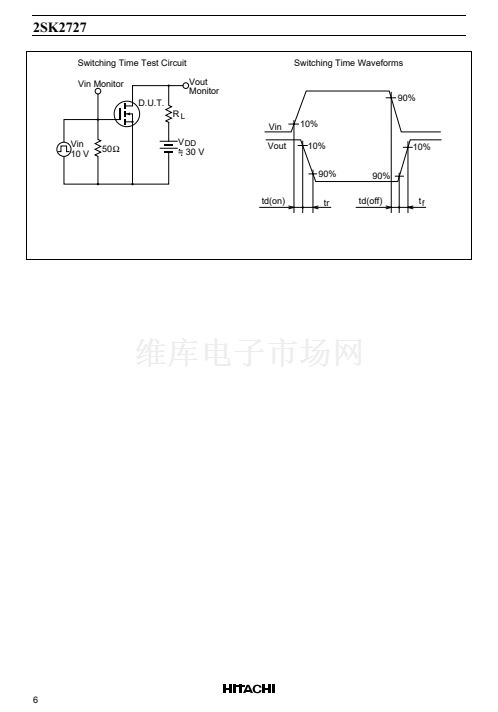
Turn-on delay time
Rise time
Turn-off delay time
Fall time
Body to drain diode forward
voltage
Body to drain diode reverse
recovery time
Note:
1. Pulse test
Qg
Qgs
Qgd
t
d(on)
t
r
t
d(off)
t
f
V
DF
t
rr
See characteristics curves of 2SK2726
3


 1
1
 2
2
 3
3
 4
4
 5
5
 6
6
 7
7
 8
8
