Philips Semiconductors
74HC164; 74HCT164
8-bit serial-in, parallel-out shift register
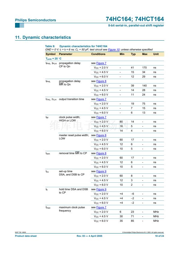
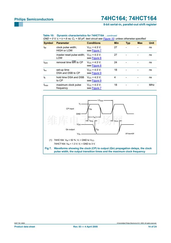
Table 10: Dynamic characteristics for 74HCT164
GND = 0 V; t
r
= t
f
= 6 ns; C
L
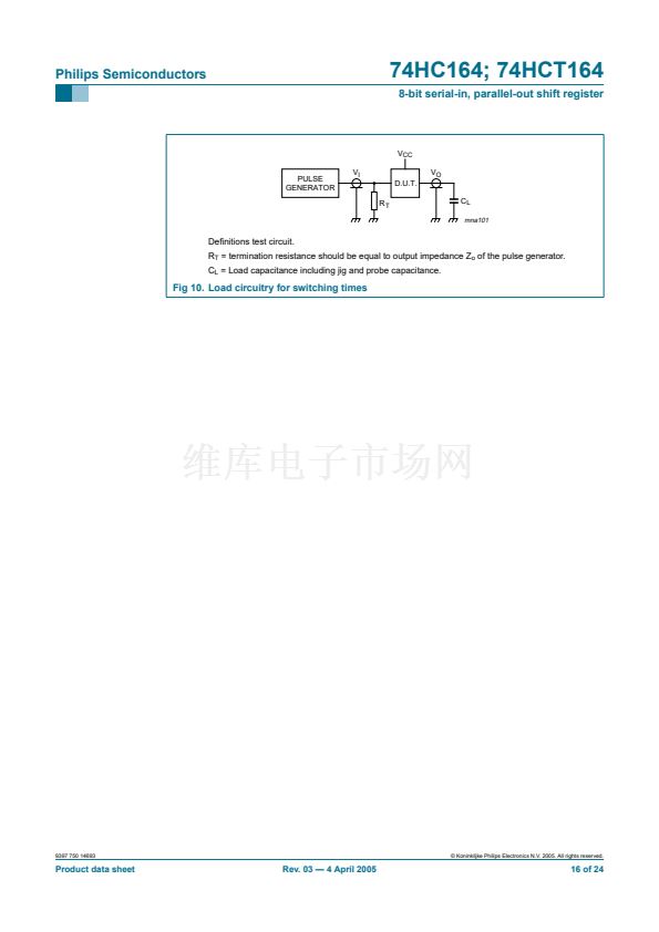
= 50 pF; test circuit see
Figure 10;
unless otherwise speci铿乪d
Symbol
Parameter
Conditions
V
CC
= 4.5 V;
see
Figure 7
V
CC
= 4.5 V;
see
Figure 8
V
CC
= 4.5 V;
see
Figure 7
V
CC
= 4.5 V;
see
Figure 7
Min
-
-
-
18
18
16
12
+4
27
Typ
17
19
7
7
10
7
6
鈭?
55
Max
36
38
15
-
-
-
-
-
-
Unit
ns
ns
ns
ns
ns
ns
ns
ns
MHz
T
amb
= 25
掳C
t
PHL
, t
PLH
propagation delay
CP to Qn
t
PHL
propagation delay
MR to Qn
t
THL
, t
TLH
output transition time
t
W
clock pulse width;
HIGH or LOW
master reset pulse width; V
CC
= 4.5 V;
see
Figure 8
LOW
t
rem
t
su
t
h
f
max
removal time MR to CP
set-up time
DSA, and DSB to CP
V
CC
= 4.5 V;
see
Figure 8
V
CC
= 4.5 V;
see
Figure 9
hold time DSA, and DSB V
CC
= 4.5 V;
to CP
see
Figure 9
maximum clock pulse
frequency
V
CC
= 4.5 V;
see
Figure 7
V
CC
= 4.5 V;
see
Figure 7
V
CC
= 4.5 V;
see
Figure 8
V
CC
= 4.5 V;
see
Figure 7
V
CC
= 4.5 V;
see
Figure 7
T
amb
=
鈭?0 掳C
to +85
掳C
t
PHL
, t
PLH
propagation delay
CP to Qn
t
PHL
propagation delay
MR to Qn
-
-
-
23
23
20
15
4
22
-
-
-
-
-
-
-
-
-
45
48
19
-
-
-
-
-
-
ns
ns
ns
ns
ns
ns
ns
ns
MHz
t
THL
, t
TLH
output transition time
t
W
clock pulse width;
HIGH or LOW
master reset pulse width; V
CC
= 4.5 V;
see
Figure 8
LOW
t
rem
t
su
t
h
f
max
removal time MR to CP
set-up time
DSA, and DSB to CP
V
CC
= 4.5 V;
see
Figure 8
V
CC
= 4.5 V;
see
Figure 9
hold time DSA, and DSB V
CC
= 4.5 V;
to CP
see
Figure 9
maximum clock pulse
frequency
V
CC
= 4.5 V;
see
Figure 7
V
CC
= 4.5 V;
see
Figure 7
V
CC
= 4.5 V;
see
Figure 8
V
CC
= 4.5 V;
see
Figure 7
T
amb
=
鈭?0 掳C
to +125
掳C
t
PHL
, t
PLH
propagation delay
CP to Qn
t
PHL
propagation delay
MR to Qn
-
-
-
-
-
-
54
57
22
ns
ns
ns
t
THL
, t
TLH
output transition time
9397 750 14693
漏 Koninklijke Philips Electronics N.V. 2005. All rights reserved.
Product data sheet
Rev. 03 鈥?4 April 2005
13 of 24


 1
1
 2
2
 3
3
 4
4
 5
5
 6
6
 7
7
 8
8
 9
9
 10
10
 11
11
 12
12
 13
13
 14
14
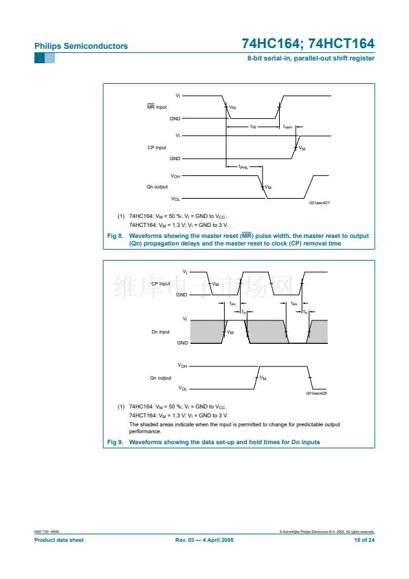 15
15
 16
16
 17
17
 18
18
 19
19
 20
20
 21
21
 22
22
 23
23
 24
24
