鈥?/div>
Direct interface with TTL levels
DESCRIPTION
The 74LVC16241A is a high-performance, low-power, low-voltage,
Si-gate CMOS device, superior to most advanced CMOS
compatible TTL families. Inputs can be driven from either 3.3V or 5V
devices. In 3-State operation, outputs can handle 5V. These
features allow the use of these devices in a mixed 3.3V/5V
environment.
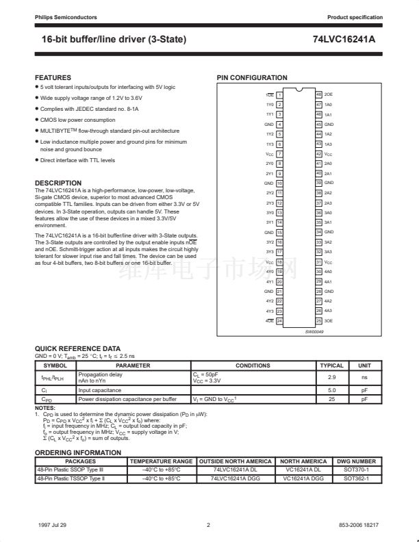
The 74LVC16241A is a 16-bit buffer/line driver with 3-State outputs.
The 3-State outputs are controlled by the output enable inputs nOE
and nOE. Schmitt-trigger action at all inputs makes the circuit highly
tolerant for slower input rise and fall times. The device can be used
as four 4-bit buffers, two 8-bit buffers or one 16-bit buffer.
GND 10
2Y2 11
2Y3 12
3Y0 13
3Y1 14
GND 15
3Y2 16
3Y3 17
V
CC
18
4Y0 19
4Y1 20
GND 21
4Y2 22
4Y3 23
4OE 24
SW00049
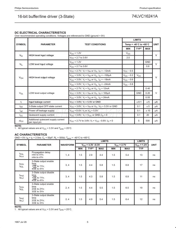
QUICK REFERENCE DATA
GND = 0 V; T
amb
= 25
_C;
t
r
= t
f
v
2.5 ns
SYMBOL
t
PHL
/t
PLH
C
I
C
PD
PARAMETER
Propagation delay
nAn to nYn
Input capacitance
Power dissipation capacitance per buffer
V
I
= GND to V
CC1
C
L
= 50pF
V
CC
= 3.3V
CONDITIONS
TYPICAL
2.9
5.0
25
UNIT
ns
pF
pF
NOTES:
1. C
PD
is used to determine the dynamic power dissipation (P
D
in
mW):
P
D
= C
PD
x V
CC2
x f
i
+
S
(C
L
x V
CC2
x f
o
) where:
f
i
= input frequency in MHz; C
L
= output load capacity in pF;
f
o
= output frequency in MHz; V
CC
= supply voltage in V;
S
(C
L
x V
CC2
x f
o
) = sum of outputs.
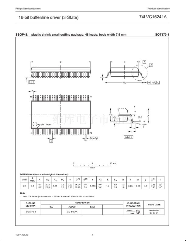
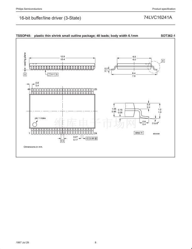
ORDERING INFORMATION
PACKAGES
48-Pin Plastic SSOP Type III
48-Pin Plastic TSSOP Type II
TEMPERATURE RANGE
鈥?0掳C to +85掳C
鈥?0掳C to +85掳C
OUTSIDE NORTH AMERICA
74LVC16241A DL
74LVC16241A DGG
NORTH AMERICA
VC16241A DL
VC16241A DGG
DWG NUMBER
SOT370-1
SOT362-1
1997 Jul 29
2
853-2006 18217


 1
1
 2
2
 3
3
 4
4
 5
5
 6
6
 7
7
 8
8
 9
9
 10
10
