Philips Semiconductors
Product specification
16-bit buffer/line driver (3-State)
74LVC16241A
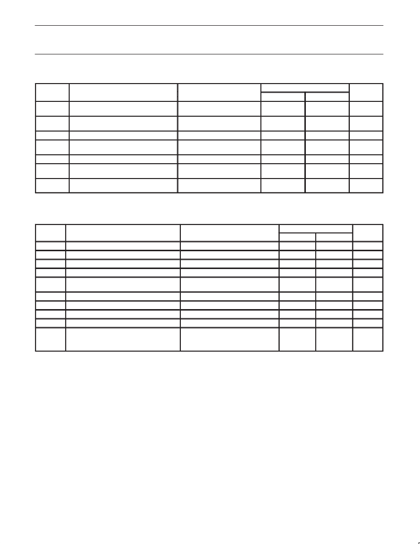
RECOMMENDED OPERATING CONDITIONS
SYMBOL
V
CC
V
CC
V
I
V
O
V
O
T
amb
t
r
, t
f
PARAMETER
DC supply voltage (for max. speed
performance)
DC supply voltage (for low-voltage
applications)
DC Input voltage range
DC output voltage range; output HIGH or
LOW state
DC output voltage range; output 3-State
Operating ambient temperature range in
free air
Input rise and fall times
See DC and AC characteristics
for individual device
V
CC
= 1.2 to 2.7V
V
CC
= 2.7 to 3.6V
CONDITIONS
LIMITS
MIN
MIN.
2.7
1.2
0
0
0
鈥?0
0
0
MAX
MAX.
3.6
3.6
5.5
V
CC
5.5
+85
20
10
UNIT
V
V
V
V
V
掳C
ns/V
ABSOLUTE MAXIMUM RATINGS
1
In accordance with the Absolute Maximum Rating System (IEC 134) Voltages are referenced to GND (ground = 0V)
SYMBOL
V
CC
I
IK
V
I
I
OK
V
O
V
O
I
O
I
GND
, I
CC
T
stg
P
tot
PARAMETER
DC supply voltage
DC input diode current
DC input voltage
DC output diode current
DC output voltage; output HIGH or LOW
state
DC output voltage; output 3-State
DC output source or sink current
DC V
CC
or GND current
Storage temperature range
Power dissipation per package
鈥?SO package
鈥?SSOP and TSSOP package
Above +70掳C derate linearly 8mW/K
Above +60掳C derate linearly 5.5mW/K
V
I
< 0
Note 2
V
O
> V
CC
or V
O
< 0
Note 2
Note 2
V
O
= 0 to V
CC
CONDITIONS
LIMITS
MIN
鈥?.5
鈥?/div>
鈥?.5
鈥?/div>
鈥?.5
鈥?.5
鈥?/div>
鈥?/div>
鈥?5
MAX
+6.5
鈥?0
+6.5
"50
V
CC
+ 0.5
6.5
"50
"100
+150
500
500
UNIT
V
mA
V
mA
V
V
mA
mA
掳C
mW
NOTES:
1. Stresses beyond those listed may cause permanent damage to the device. These are stress ratings only and functional operation of the
device at these or any other conditions beyond those indicated under 鈥渞ecommended operating conditions鈥?is not implied. Exposure to
absolute-maximum-rated conditions for extended periods may affect device reliability.
2. The input and output voltage ratings may be exceeded if the input and output clamp current ratings are observed.
1997 Jul 29
4


 1
1
 2
2
 3
3
 4
4
 5
5
 6
6
 7
7
 8
8
 9
9
 10
10
