Philips Semiconductors
Product specification
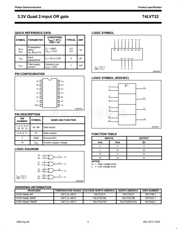
3.3V Quad 2-input OR gate
74LVT32
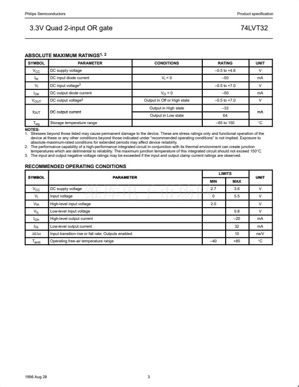
ABSOLUTE MAXIMUM RATINGS
1, 2
SYMBOL
V
CC
I
IK
V
I
I
OK
V
OUT
I
OUT
T
stg
PARAMETER
DC supply voltage
DC input diode current
DC input voltage
3
DC output diode current
DC output voltage
3
DC output current
Output in Low state
Storage temperature range
64
鈥?5 to 150
掳C
V
O
< 0
Output in Off or High state
Output in High state
V
I
< 0
CONDITIONS
RATING
鈥?.5 to +4.6
鈥?0
鈥?.5 to +7.0
鈥?0
鈥?.5 to +7.0
鈥?2
mA
UNIT
V
mA
V
mA
V
NOTES:
1. Stresses beyond those listed may cause permanent damage to the device. These are stress ratings only and functional operation of the
device at these or any other conditions beyond those indicated under 鈥渞ecommended operating conditions鈥?is not implied. Exposure to
absolute-maximum-rated conditions for extended periods may affect device reliability.
2. The performance capability of a high-performance integrated circuit in conjunction with its thermal environment can create junction
temperatures which are detrimental to reliability. The maximum junction temperature of this integrated circuit should not exceed 150掳C.
3. The input and output negative voltage ratings may be exceeded if the input and output clamp current ratings are observed.
RECOMMENDED OPERATING CONDITIONS
LIMITS
SYMBOL
V
CC
V
I
V
IH
V
IL
I
OH
I
OL
鈭唗/鈭唙
T
amb
DC supply voltage
Input voltage
High-level input voltage
Low-level Input voltage
High-level output current
Low-level output current
Input transition rise or fall rate; Outputs enabled
Operating free-air temperature range
鈥?0
PARAMETER
MIN
2.7
0
2.0
0.8
鈥?0
32
10
+85
MAX
3.6
5.5
V
V
V
V
mA
mA
ns/V
掳C
UNIT
1996 Aug 28
3


 1
1
 2
2
 3
3
 4
4
 5
5
 6
6
 7
7
 8
8
 9
9
 10
10
