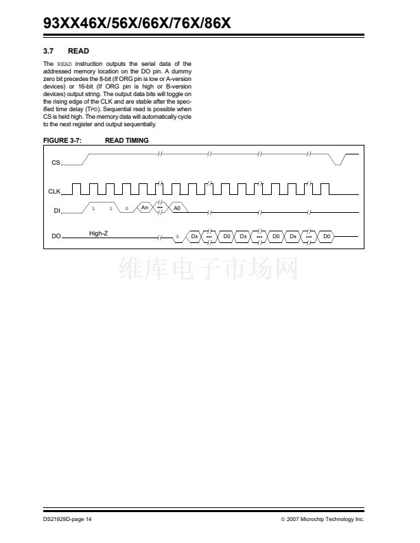
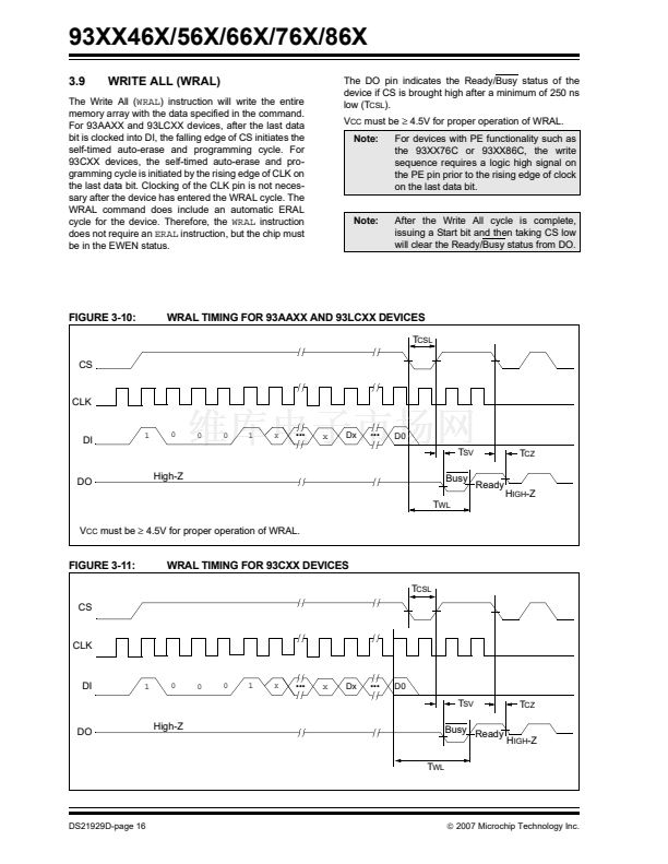
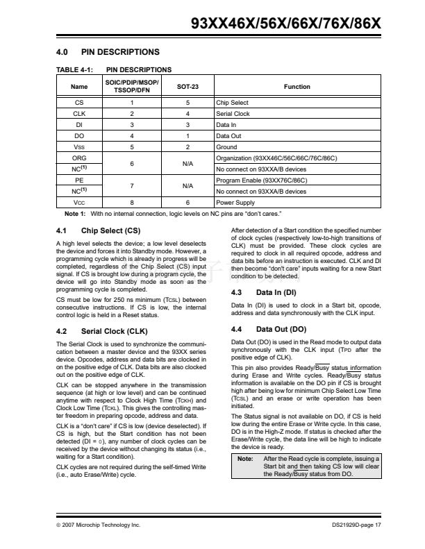
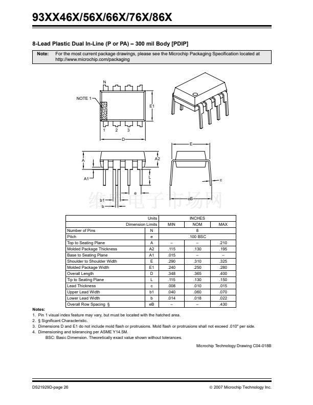
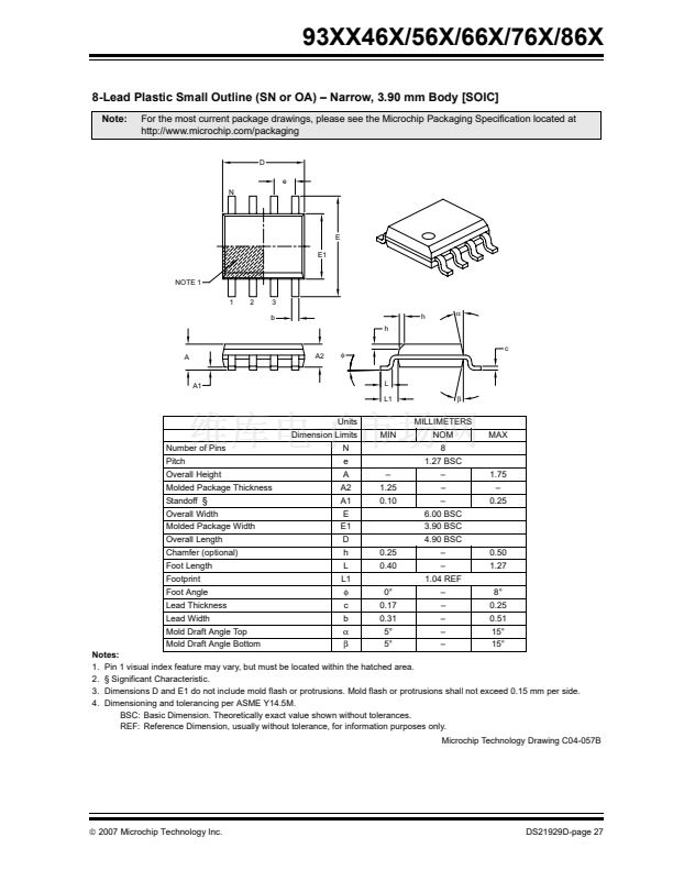
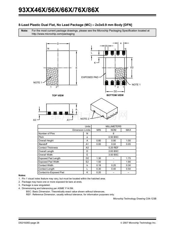
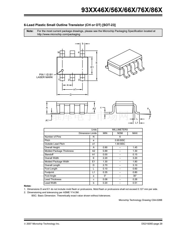
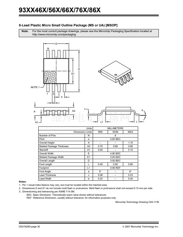
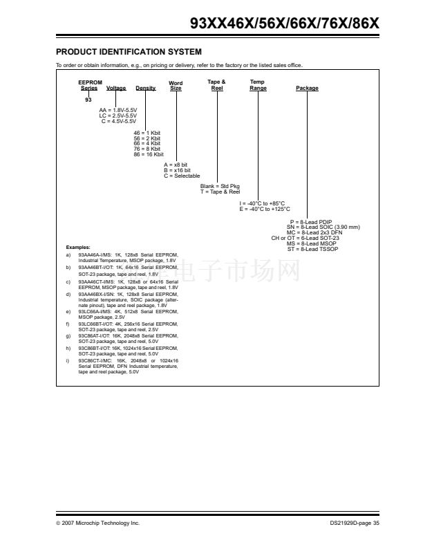
93XX46X/56X/66X/76X/86X
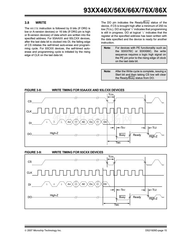
3.8
WRITE
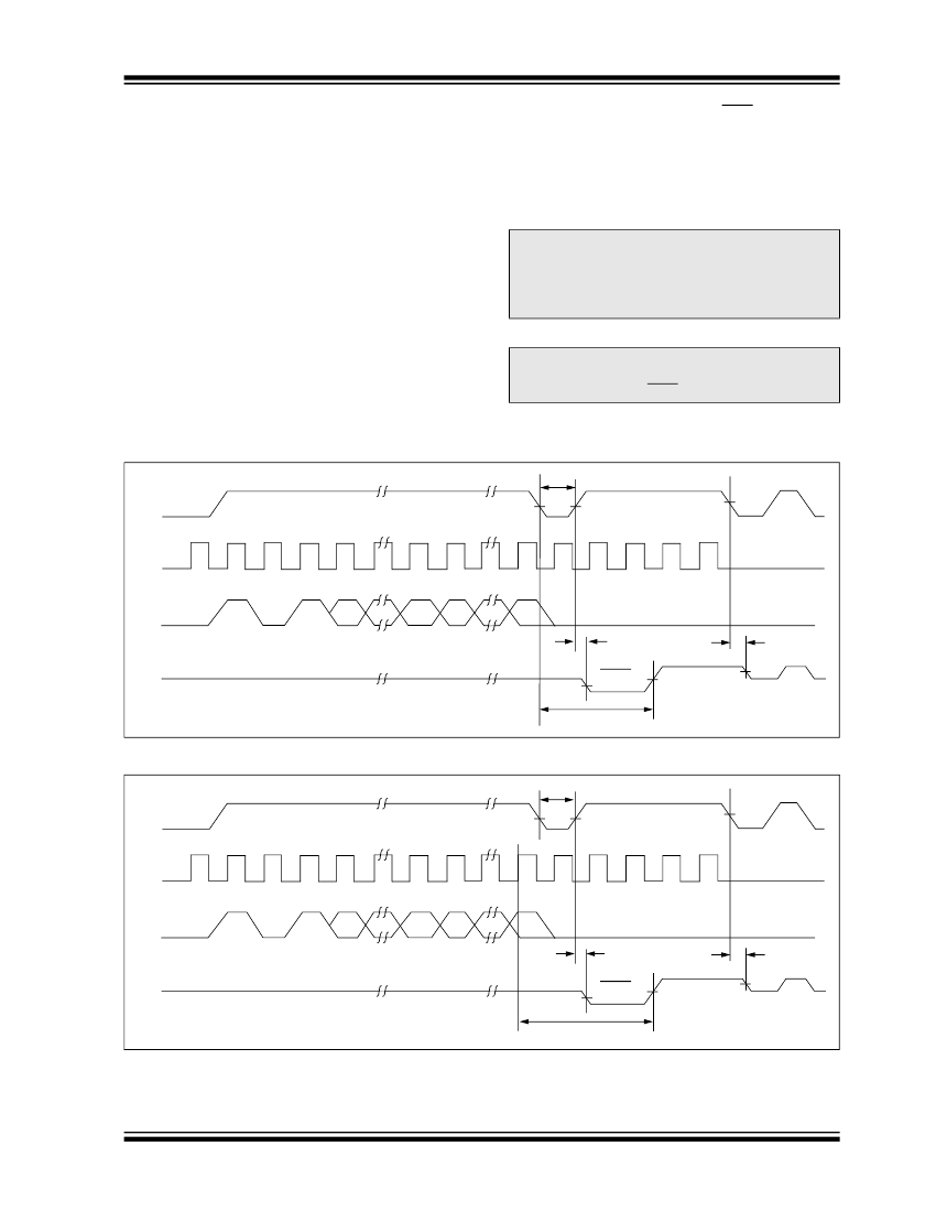
The
WRITE
instruction is followed by 8 bits (If ORG is
low or A-version devices) or 16 bits (If ORG pin is high
or B-version devices) of data which are written into the
specified address. For 93AAXX and 93LCXX devices,
after the last data bit is clocked into DI, the falling edge
of CS initiates the self-timed auto-erase and program-
ming cycle. For 93CXX devices, the self-timed auto-
erase and programming cycle is initiated by the rising
edge of CLK on the last data bit.
The DO pin indicates the Ready/Busy status of the
device, if CS is brought high after a minimum of 250 ns
low (T
CSL
). DO at logical 鈥?鈥?indicates that programming
is still in progress. DO at logical 鈥?鈥?indicates that the
register at the specified address has been written with
the data specified and the device is ready for another
instruction.
Note:
For devices with PE functionality such as
the 93XX76C or 93XX86C, the write
sequence requires a logic high signal on
the PE pin prior to the rising edge of clock
on the last data bit.
Note:
After the Write cycle is complete, issuing a
Start bit and then taking CS low will clear
the Ready/Busy status from DO.
FIGURE 3-8:
WRITE TIMING FOR 93AAXX AND 93LCXX DEVICES
T
CSL
CS
CLK
DI
1
0
1
An
鈥⑩€⑩€?/div>
A0
Dx
鈥⑩€⑩€?/div>
D0
T
SV
DO
High-Z
Busy
Twc
Ready
T
CZ
High-Z
FIGURE 3-9:
CS
WRITE TIMING FOR 93CXX DEVICES
T
CSL
CLK
DI
1
0
1
An
鈥⑩€⑩€?/div>
A0
Dx
鈥⑩€⑩€?/div>
D0
T
SV
DO
High-Z
Busy
Twc
Ready
T
CZ
High-Z
漏
2007 Microchip Technology Inc.
DS21929D-page 15


 1
1
 2
2
 3
3
 4
4
 5
5
 6
6
 7
7
 8
8
 9
9
 10
10
 11
11
 12
12
 13
13
 14
14
 15
15
 16
16
 17
17
 18
18
 19
19
 20
20
 21
21
 22
22
 23
23
 24
24
 25
25
 26
26
 27
27
 28
28
 29
29
 30
30
 31
31
 32
32
 33
33
 34
34
 35
35
 36
36
 37
37
 38
38
