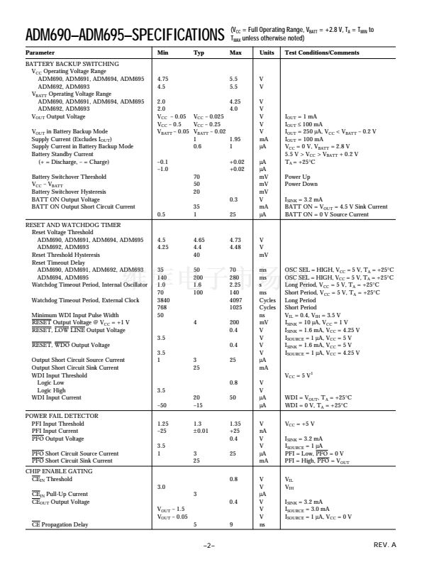
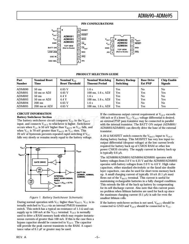
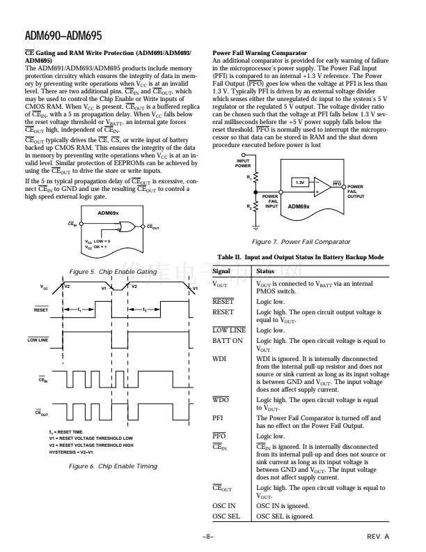
to whichever is higher. Switchover
rises. This
falls very slowly or remains nearly equal to the battery voltage.
with the internal transistor. The BATT ON output (ADM691/
transistor.
鈩?/div>
MOSFET switch connects the V
BATT
input to V
OUT
during battery backup. This MOSFET has very low input-to-
output differential (dropout voltage) at the low current levels
required for battery back up of CMOS RAM or other low
power CMOS circuitry. The supply current in battery back up
is typically 0.6
碌A.
The ADM690/ADM691/ADM694/ADM695 operates with
battery voltages from 2.0 V to 4.25 V and the ADM692/ADM693
operates with battery voltages from 2.0 V to 4.0 V. High value
capacitors, either standard electrolytic or the farad size double
layer capacitors, can also be used for short-term memory back
up. A small charging current of typically 10 nA (0.1
碌A
max)
flows out of the V
BATT
terminal. This current is useful for
maintaining rechargeable batteries in a fully charged condition.
This extends the life of the back up battery by compensating
for its self discharge current. Also note that this current poses
no problem when lithium batteries are used for back up since
the maximum charging current (0.1
碌A)
is safe for even the
smallest lithium cells.
If the battery-switchover section is not used, V
BATT
should be
connected to GND and V
OUT
should be connected to V
CC
.
Figure 1. Battery Switchover Schematic
During normal operation with V
CC
higher than V
BATT
, V
CC
is in-
ternally switched to V
OUT
via an internal PMOS transistor
switch. This switch has a typical on-resistance of 1.5
鈩?/div>
and can
supply up to 100 mA at the V
OUT
terminal. V
OUT
is normally
used to drive a RAM memory bank which may require instanta-
neous currents of greater than 100 mA. If this is the case then a
bypass capacitor should be connected to V
OUT
. The capacitor
will provide the peak current transients to the RAM. A capaci-
tance value of 0.1
碌F
or greater may be used.
REV. A
鈥?鈥?/div>
prev
next


 1
1
 2
2
 3
3
 4
4
 5
5
 6
6
 7
7
 8
8
 9
9
 10
10
 11
11
 12
12
 13
13
 14
14
 15
15
 16
16
