CED73A3/CEU73A3
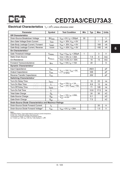
Electrical Characteristics
Parameter
Off Characteristics
Drain-Source Breakdown Voltage
Zero Gate Voltage Drain Current
Gate Body Leakage Current, Forward
Gate Body Leakage Current, Reverse
On Characteristics
Static Drain-Source
On-Resistance
Forwand Transconductance
Dynamic Characteristics
Input Capacitance
Output Capacitance
Reverse Transfer Capacitance
Switching Characteristics
Turn-On Delay Time
Turn-On Rise Time
Turn-Off Delay Time
Turn-On Fall Time
Total Gate Charge
Gate-Source Charge
Gate-Drain Charge
Drain-Source Diode Forward Current
Drain-Source Diode Forward Voltage
b
c
c
b
Tc = 25 C unless otherwise noted
Symbol
BV
DSS
I
DSS
I
GSSF
I
GSSR
V
GS(th)
R
DS(on)
g
FS
C
iss
C
oss
C
rss
t
d(on)
t
r
t
d(off)
t
f
Q
g
Q
gs
Q
gd
I
S
V
SD
V
GS
= 0V, I
S
= 20A
V
DS
= 15V, I
D
= 20A,
V
GS
= 4.5V
V
DD
= 15V, I
D
= 1A,
V
GS
= 10V, R
GEN
= 6鈩?/div>
Test Condition
V
GS
= 0V, I
D
= 250碌A
V
DS
= 25V, V
GS
= 0V
V
GS
= 20V, V
DS
= 0V
V
GS
= -20V, V
DS
= 0V
V
GS
= V
DS
, I
D
= 250碌A
V
GS
= 10V, I
D
= 30A
V
GS
= 4.5V, I
D
= 30A
V
DS
= 10V, I
D
= 15A
1
7.8
10
20
2923
506
202
19
6.8
71
12.8
24
9.1
7.5
20
1.5
23
12
128
17.5
30
Min
30
1
100
-100
3
9
13
Typ
Max
Units
V
碌A
nA
nA
V
m鈩?/div>
m鈩?/div>
S
pF
pF
pF
ns
ns
ns
ns
nC
nC
nC
A
V
6
Gate Threshold Voltage
V
DS
= 15V, V
GS
= 0V,
f = 1.0 MHz
Drain-Source Diode Characteristics and Maximun Ratings
Notes :
a.Repetitive Rating : Pulse width limited by maximum junction temperature.
b.Pulse Test : Pulse Width < 300碌s, Duty Cycle < 2%.
c.Guaranteed by design, not subject to production testing.
d.L = 0.5mH, I
AS
= 25A, V
DD
= 24V, R
G
= 25鈩? Starting T
J
= 25 C
6 - 123


 1
1
 2
2
 3
3
 4
4
