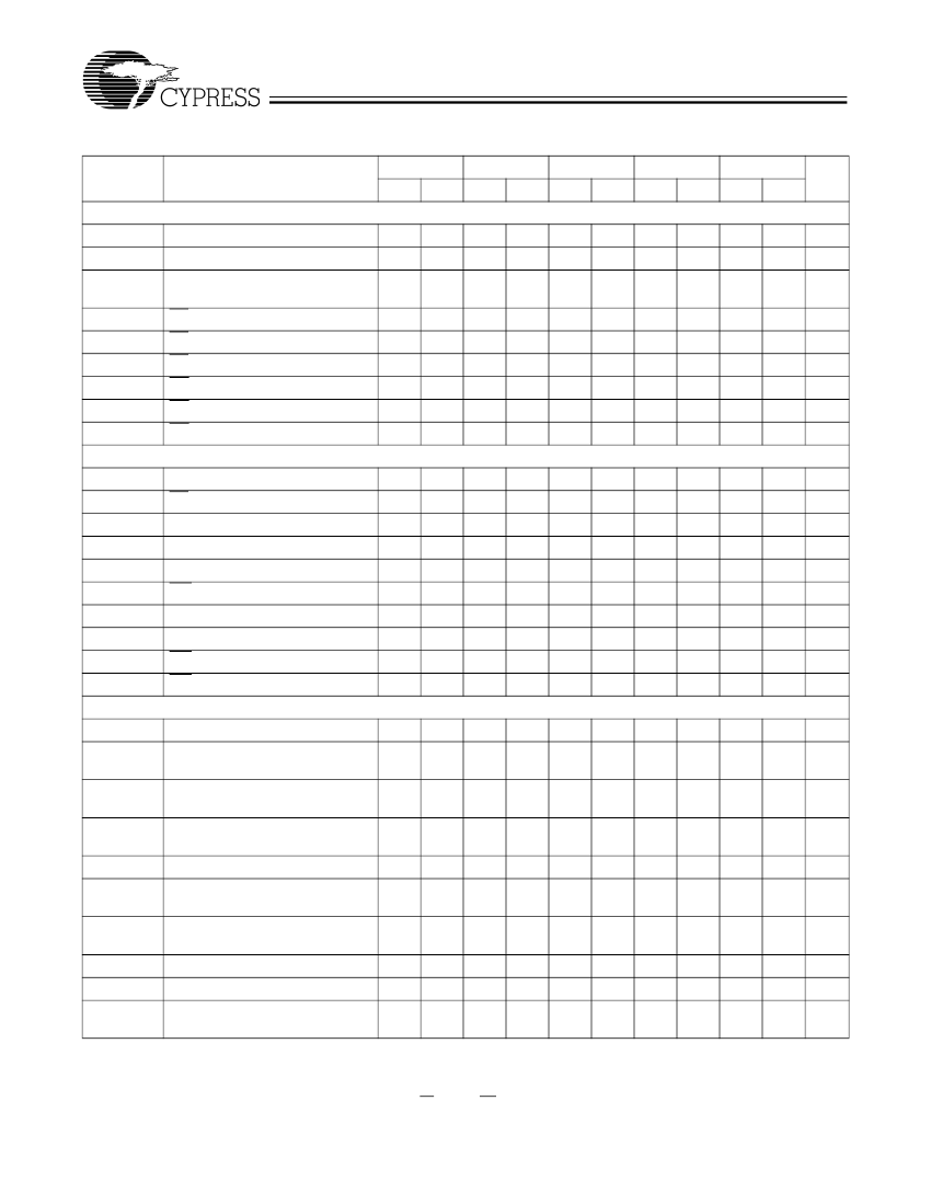
CY7C150
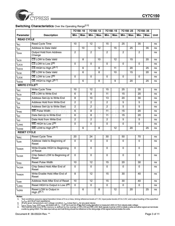
Switching Characteristics
Over the Operating Range
[2,5]
7C150鈭?0
Parameter
READ CYCLE
t
RC
t
AA
t
OHA
t
ACS
t
LZCS
t
HZCS
t
DOE
t
LZOE
t
HZOE
t
WC
t
SCS
t
AW
t
HA
t
SA
t
PWE
t
SD
t
HD
t
LZWE
t
HZWE
t
RRC
t
SAR
t
SWER
t
SCSR
t
PRS
t
HCSR
t
HWER
t
HAR
t
LZRS
t
HZRS
Read Cycle Time
Address to Data Valid
Output Hold from Address
Change
CS LOW to Data Valid
CS LOW to Low Z
[6]
CS HIGH to High Z
[6,7]
OE LOW to Data Valid
OE LOW to Low Z
[6]
7C150鈭?2
Min.
12
Max.
7C150鈭?5
Min.
15
Max.
7C150鈭?5
Min.
25
Max.
7C150鈭?5
Min.
35
Max.
Unit
ns
35
2
ns
ns
20
0
25
20
0
25
35
20
30
5
5
20
20
5
0
ns
ns
ns
ns
ns
ns
ns
ns
ns
ns
ns
ns
ns
ns
ns
25
70
0
0
0
30
0
40
40
0
ns
ns
ns
ns
ns
ns
ns
ns
ns
ns
25
ns
Description
Min.
10
Max.
10
2
8
0
6
6
0
6
10
6
8
2
2
6
6
2
0
6
20
0
0
0
10
0
8
10
0
6
24
0
0
0
12
0
12
12
0
12
8
10
2
2
8
8
2
0
0
0
2
12
2
10
0
8
8
0
8
15
11
13
2
2
11
11
2
0
8
30
0
0
0
15
0
15
15
0
8
15
2
12
0
11
10
0
9
25
15
20
5
5
15
15
5
0
12
50
0
0
0
20
0
30
30
0
12
25
15
20
15
20
OE HIGH to High Z
[6,7]
Write Cycle Time
CS LOW to Write End
Address Set-Up to Write End
Address Hold from Write End
Address Set-Up to Write Start
WE Pulse Width
Data Set-Up to Write End
Data Hold from Write End
WE HIGH to Low Z
[6]
WE LOW to High Z
[6,7]
Reset Cycle Time
Address Valid to Beginning of
Reset
Write Enable HIGH to Beginning
of Reset
Chip Select LOW to Beginning of
Reset
Reset Pulse Width
Chip Select Hold After End of
Reset
Write Enable Hold After End of
Reset
Address Hold After End of Reset
Reset HIGH to Output in Low Z
[6]
Reset LOW to Output in
High Z
[6,7]
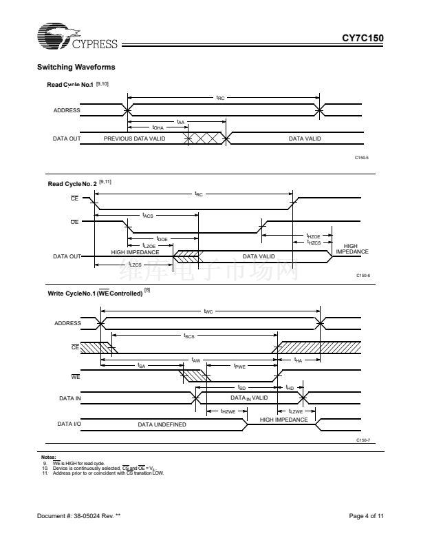
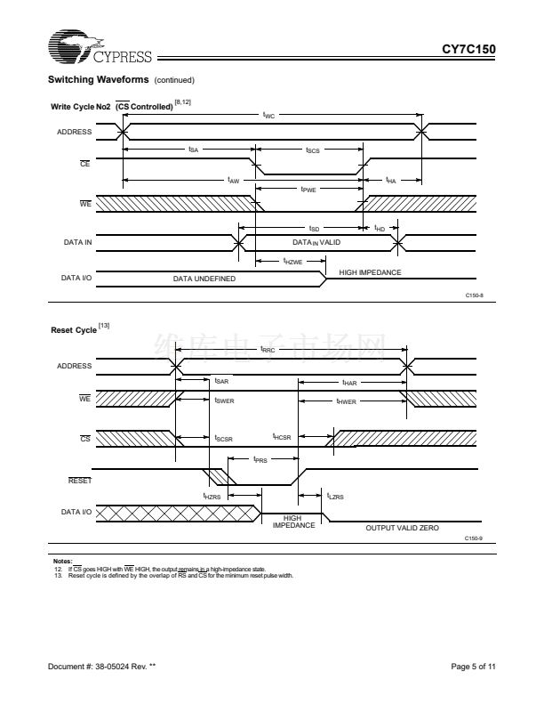
WRITE CYCLE
[8]
20
RESET CYCLE
20
Notes:
5. Test conditions assume signal transition times of 5 ns or less, timing reference levels of 1.5V, input pulse levels of 0 to 3.0V, and output loading of the specified
I
OL
/I
OH
and 30-pF load capacitance.
6. At any given temperature and voltage condition, t
HZ
is less than t
LZ
for any given device.
7. t
HZCS
, t
HZOE
, t
HZR
, and t
HZWE
are tested with C
L
= 5 pF as in part (b) of AC Test Loads. Transition is measured
卤
500 mV from steady-state voltage.
8. The internal write time of the memory is defined by the overlap of CS LOW and WE LOW. Both signals must be LOW to initiate a write and either signal can terminate
a write by going HIGH. The data input set-up and hold timing should be reference to the rising edge of the signal that terminates the write.
Document #: 38-05024 Rev. **
Page 3 of 11


 1
1
 2
2
 3
3
 4
4
 5
5
 6
6
 7
7
 8
8
 9
9
 10
10
 11
11
