ICL232
Pin Descriptions
PDIP, CERDIP
9
10
11
12
13
14
15
16
(Continued)
SOIC
9
10
11
12
13
14
15
16
PIN NAME
R2out
T2
IN
T1
IN
R1
OUT
R1
IN
T1
OUT
GND
V
CC
Receiver 2 TTL/CMOS output.
Transmitter 2 TTL/CMOS input, with internal 400K pullup resistor to V
CC
.
Transmitter 1 TTL/CMOS input, with internal 400K pullup resistor to V
CC
.
Receiver 1 TTL/CMOS output.
RS-232 Receiver 1 input, with internal 5K pulldown resistor to GND.
RS-232 Transmitter 1 output
卤10V
(typical).
Supply Ground.
Positive Power Supply +5V
卤10%
DESCRIPTION
VOLTAGE DOUBLER
S1
V
CC
+
C1
+
S2
+
V+ = 2V
CC
C3
V
CC
GND
S7
S5
VOLTAGE INVERTER
C2
+
+
S6
GND
+
-
GND
S3
C1
-
C1
S4
-
-
C2
-
C2
-
S8
C4
V- = -(V+)
RC
OSCILLATOR
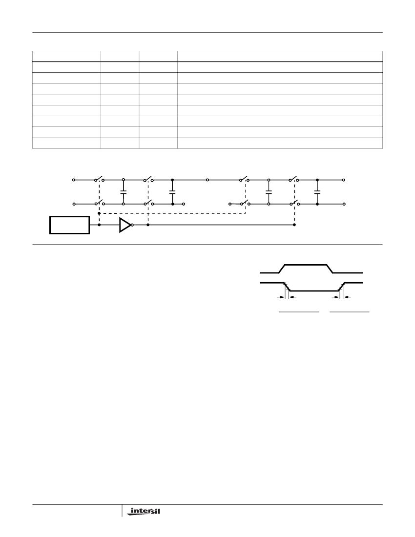
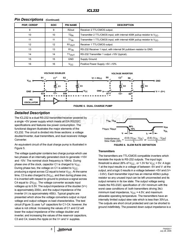
FIGURE 5. DUAL CHARGE PUMP
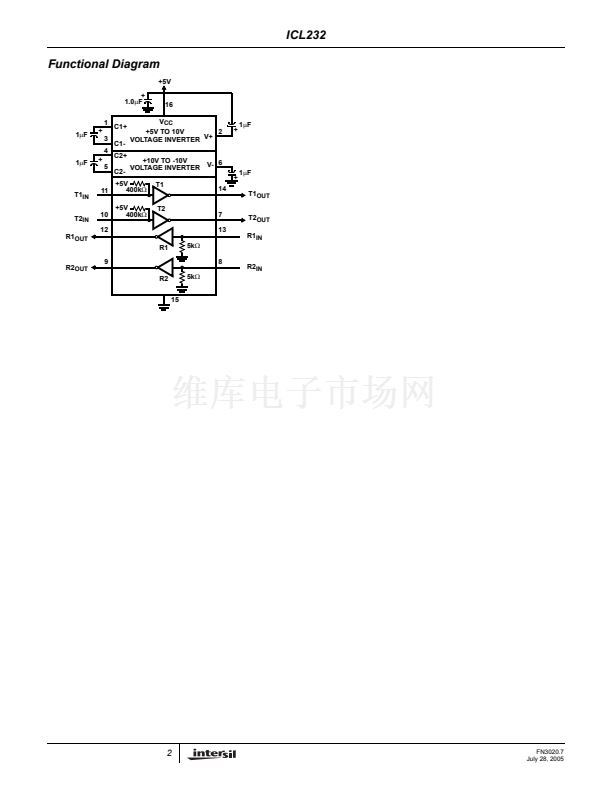
Detailed Description
The ICL232 is a dual RS-232 transmitter/receiver powered by
a single +5V power supply which meets all ElA RS232C
specifications and features low power consumption. The
functional diagram illustrates the major elements of the
ICL232. The circuit is divided into three sections: a voltage
doubler/inverter, dual transmitters, and dual receivers Voltage
Converter.
An equivalent circuit of the dual charge pump is illustrated in
Figure 5.
The voltage quadrupler contains two charge pumps which use
two phases of an internally generated clock to generate +10V
and -10V. The nominal clock frequency is 16kHz. During
phase one of the clock, capacitor C1 is charged to V
CC
.
During phase two, the voltage on C1 is added to V
CC
,
producing a signal across C2 equal to twice V
CC
. At the same
time, C3 is also charged to 2V
CC
, and then during phase one,
it is inverted with respect to ground to produce a signal across
C4 equal to -2V
CC
. The voltage converter accepts input
voltages up to 5.5V. The output impedance of the doubler (V+)
is approximately 200鈩? and the output impedance of the
inverter (V-) is approximately 450鈩? Typical graphs are
presented which show the voltage converters output vs input
voltage and output voltages vs load characteristics. The test
circuit (Figure 3) uses 1碌F capacitors for C1-C4, however, the
value is not critical. Increasing the values of C1 and C2 will
lower the output impedance of the voltage doubler and
inverter, and increasing the values of the reservoir capacitors,
C3 and C4, lowers the ripple on the V+ and V- supplies.
T1
IN
, T2
IN
T1
OUT
, T2
OUT
t
f
90%
10%
t
r
V
OH
V
OL
(0.8) (V
OH
- V
OL
)
(0.8) (V
OL
- V
OH
)
Instantaneous
=
or
Slew Rate (SR)
t
r
t
f
FIGURE 6. SLEW RATE DEFINITION
Transmitters
The transmitters are TTL/CMOS compatible inverters which
translate the inputs to RS-232 outputs. The input logic
threshold is about 26% of V
CC
, or 1.3V for V
CC
= 5V. A logic
1 at the input results in a voltage of between -5V and V- at the
output, and a logic 0 results in a voltage between +5V and (V+
- 0.6V). Each transmitter input has an internal 400k鈩?pullup
resistor so any unused input can be left unconnected and its
output remains in its low state. The output voltage swing
meets the RS-232C specification of
卤5V
minimum with the
worst case conditions of: both transmitters driving 3k鈩?/div>
minimum load impedance, V
CC
= 4.5V, and maximum
allowable operating temperature. The transmitters have an
internally limited output slew rate which is less than 30V/碌s.
The outputs are short circuit protected and can be shorted to
ground indefinitely. The powered down output impedance is a
5
FN3020.7
July 28, 2005


 1
1
 2
2
 3
3
 4
4
 5
5
 6
6
 7
7
