MAX2360 Evaluation Kit
Evaluates: MAX2360/MAX2362/MAX2364
spectrum analyzer to measure ACPR for reverse-
channel CDMA. Set the center frequency to
836MHz with a +10dBm reference level.
12) The output power should be about 7dBm after
accounting for cable and connector loss. The ACPR
at 卤885kHz offset should be -54dBc, and the ACPR
at 卤1.98MHz offset should be -70dBc.
Low-Band PCS CDMA Mode
Perform the following steps to evaluate the MAX2360 in
the PCS CDMA mode:
1) Connect the PCS VCO module side of JU3 to the
low-noise power supply or a regulator.
2) With the MAX2360 control screen active, click on
the PCS Low preset located at the left of the screen.
3) Click on the Send Data buttons for each of the con-
trol registers located at the right of the screen.
There are seven registers that need to be down-
loaded to the IC. The Lock LED on the screen
should be red, indicating lock.
4) Set the VGA control to 2.55VDC by rotating poten-
tiometer R66. Optionally, an external VGA control
voltage may be used by removing jumper JU4 and
applying a DC voltage to header VGC. Current con-
sumption is about 150mA. This includes the RF
VCO and the potentiometer.
5) Connect the RFH1 port to the spectrum analyzer.
Configure a spectrum analyzer to measure ACPR
for reverse-channel CDMA. Set the center frequen-
cy to 1880.38 MHz with a +10dBm reference level.
6) The output power should be about 7dBm after
accounting for cable and connector loss. The ACPR
at 卤1.25MHz offset should be -54dBc.
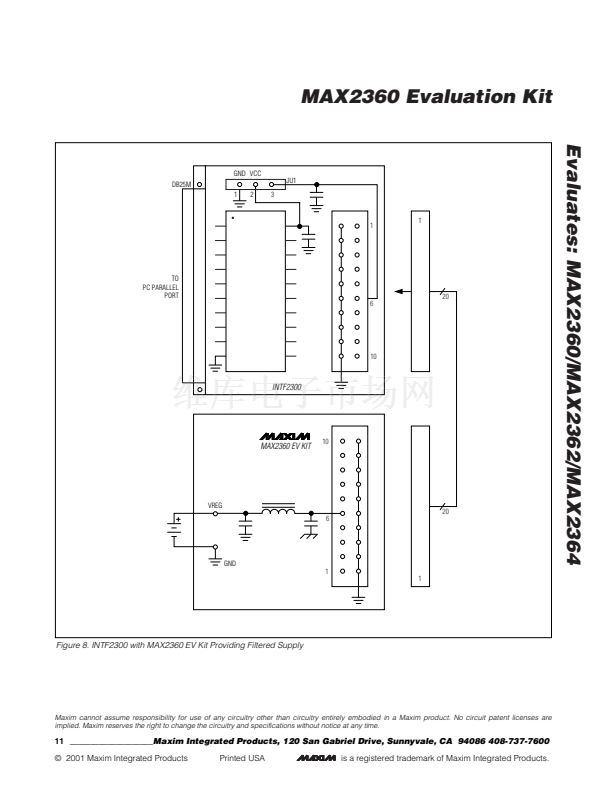
Interface Control
The interface port is designed to use a 20-pin ribbon
cable (Figure 8); 10 pins are signal lines, and the other
10 pins are digital grounds. Pin 1 of the interface cable
is red. Pin 1 is also designated in silk screen on each of
the PC boards.
IDLE
A logic low on the
IDLE
pin shuts down everything
except the RF PLL and associated registers.
TXGATE
A logic low on the
TXGATE
pin shuts down everything
except the RF PLL, IF PLL, IF VCO, serial bus, and reg-
isters. This mode is used for gated transmission.
SHDN
A logic low on the
SHDN
pin powers down the entire
device, including registers and the serial interface.
Detailed Description
The following section covers the EV kit鈥檚 circuit blocks
in detail (refer to the MAX2360/MAX2362/MAX2364
data sheet for additional information).
I/Q Inputs
The I/Q ports are high-impedance differential baseband
inputs. They require a DC bias level of 1/2 V
CC
with
6碌A of current drive. For convenience, the MAX2360 EV
kit provides a transformer that provides a single-ended
to differential conversion and provides bias for the I/Q
inputs. The transformer makes it easy to interface with
single-ended test equipment, but due to its low-frequen-
cy cutoff of 50kHz, does not allow full evaluation of the
MAX2360. To evaluate the part over its full bandwidth,
use shielded twisted-pair transmission line to connect a
differential signal source to the differential pads provided
on the EV kit. Stuff R10, R12, R15, and R17 with 0鈩?resis-
tors and remove R6, R8, R14, and R16 when using the
differential pads.
Adjustments and Control
VGA Adjust
The MAX2360 EV kit is configured with a 10k鈩?trim pot-
entiometer for setting and adjusting the VGA gain. By
removing the two-pin shunt JU4, an external supply can
be used by directly connecting to header VGC. The
VGC voltage is filtered on the EV kit to minimize unde-
sired amplitude modulation.
Programming Interface
The programming interface is provided by the
INTF2300 interface board. The interface board buffers
and level shifts logic levels from the PC to the MAX2360
EV kit (refer to the INTF2300 documentation). These
logic signals control the logic pins as well as the
MAX2360 serial interface.
Optional VCO External Adjust
The MAX2360 EV kit is configured with a 10k鈩?trim pot-
entiometer for setting and adjusting the VCO tune volt-
age. Apply a two-pin shunt to JU1. Stuff a 0鈩?resistor
for R33, and remove R38 to break the loop and remove
the charge-pump output. The VCO voltage must be
clean to minimize undesired frequency modulation.
IFLO
The IFLO output port provides an output signal that is
either the IF VCO frequency or the VCO frequency
divided by 2, depending on the setting of the BUF_DIV
control bit. It can be disabled by setting the BUF_EN bit
to 0 in the OPCTRL register.
4
_______________________________________________________________________________________


 1
1
 2
2
 3
3
 4
4
 5
5
 6
6
 7
7
 8
8
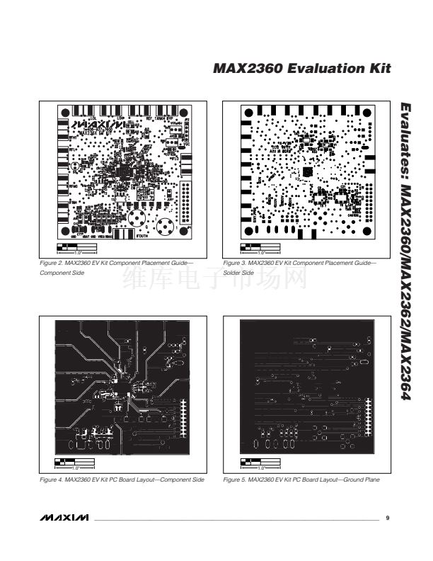 9
9
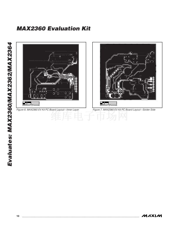 10
10
 11
11
