卤15kV ESD-Protected, 3.3V Quad
RS-422 Transmitters
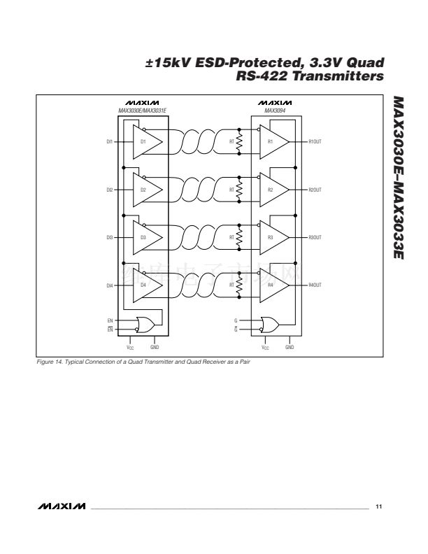
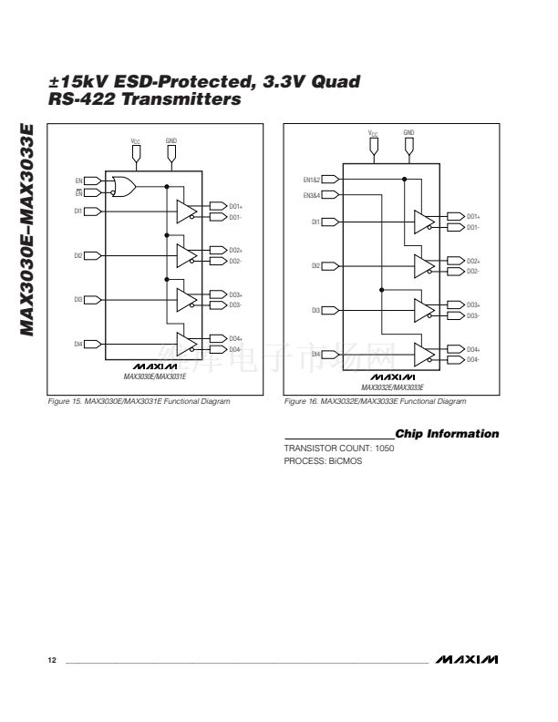
MAX3030E鈥揗AX3033E
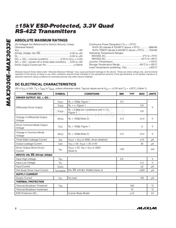
ABSOLUTE MAXIMUM RATINGS
(All Voltages Are Referenced to Device Ground, Unless
Otherwise Noted)
V
CC
........................................................................................+6V
EN1&2, EN3&4, EN,
EN............................................-0.3V
to +6V
DI_ ............................................................................-0.3V to +6V
DO_+, DO_- (normal condition) .................-0.3V to (V
CC
+ 0.3V)
DO_+, DO_- (power-off or three-state condition).....-0.3V to +6V
Driver Output Current per Pin.........................................卤150mA
Continuous Power Dissipation (T
A
= +70掳C)
16-Pin SO (derate 8.70mW/掳C above +70掳C)..............696mW
16-Pin TSSOP (derate 9.40mW/掳C above +70掳C) .......755mW
Operating Temperature Ranges
MAX303_EC_ ......................................................0掳C to +70掳C
MAX303_EE_ ...................................................-40掳C to +85掳C
Junction Temperature ......................................................+150掳C
Storage Temperature Range .............................-65掳C to +160掳C
Lead Temperature (soldering, 10s) .................................+300掳C
Stresses beyond those listed under 鈥淎bsolute Maximum Ratings鈥?may cause permanent damage to the device. These are stress ratings only, and functional
operation of the device at these or any other conditions beyond those indicated in the operational sections of the specifications is not implied. Exposure to
absolute maximum rating conditions for extended periods may affect device reliability.
DC ELECTRICAL CHARACTERISTICS
(3V
鈮?/div>
V
CC
鈮?/div>
3.6V, T
A
= T
MIN
to T
MAX
, unless otherwise noted. Typical values are at V
CC
= +3.3V and T
A
= +25掳C.) (Note 1)
PARAMETER
DRIVER OUTPUT: DO_+, DO_-
V
OD1
Differential Driver Output
V
OD2
V
OD3
Change in Differential Output
Voltage
Driver Common-Mode Output
Voltage
Change in Common-Mode
Voltage
Three-State Leakage Current
Output Leakage Current
Driver Output Short-Circuit
Current
INPUTS: EN,
EN,
EN1&2, EN3&4
Input High Voltage
Input Low Voltage
Input Current
Hot-Swap Driver Input Current
SUPPLY CURRENT
Supply Current
THERMAL PROTECTION
Thermal-Shutdown Threshold
Thermal-Shutdown Hysteresis
ESD Protection DO_
Human Body Model
T
SH
160
10
卤15
掳C
掳C
kV
I
CC
No load
100
碌A
V
IH
V
IL
I
LEAK
I
HOTSWAP
EN,
EN,
EN1&2, EN3&4 (Note 4)
2.0
0.4
卤2
卤200
V
V
碌A
碌A
鈭哣
OD
V
OC
鈭哣
OC
I
OZ
I
OFF
I
SC
R
L
= 100鈩? Figure 1
R
L
=
鈭?
Figure 1
R
L
= 3.9k鈩?(for compliance with V.11),
Figure 1
R
L
= 100鈩?(Note 2)
R
L
= 100鈩? Figure 1
R
L
= 100鈩?(Note 2)
V
OUT
= V
CC
or GND, driver disabled
V
CC
= 0V, V
OUT
= 3V or 6V
V
OUT
= 0V, V
IN
= V
CC
or GND
(Note 3)
-150
-0.4
-0.4
2.0
3.6
3.6
+0.4
3
+0.4
卤10
20
V
V
V
碌A
碌A
mA
V
SYMBOL
CONDITIONS
MIN
TYP
MAX
UNITS
2
_______________________________________________________________________________________


 1
1
 2
2
 3
3
 4
4
 5
5
 6
6
 7
7
 8
8
 9
9
 10
10
 11
11
 12
12
 13
13
 14
14
