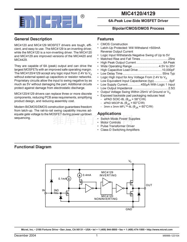
MIC4120/4129
Capacitive Load Power Dissipation
Dissipation caused by a capacitive load is simply the energy
placed in, or removed from, the load capacitance by the
driver. The energy stored in a capacitor is described by the
equation:
E = 1/2 C V
2
As this energy is lost in the driver each time the load is charged
or discharged, for power dissipation calculations the 1/2 is
removed. This equation also shows that it is good practice
not to place more voltage on the capacitor than is necessary,
as dissipation increases as the square of the voltage applied
to the capacitor. For a driver with a capacitive load:
P
L
= f C (V
S
)
2
where:
f = Operating Frequency
C = Load Capacitance
V
S
=Driver Supply Voltage
Inductive Load Power Dissipation
For inductive loads the situation is more complicated. For
the part of the cycle in which the driver is actively forcing
current into the inductor, the situation is the same as it is in
the resistive case:
P
L1
= I
2
R
O
D
However, in this instance the R
O
required may be either
the on resistance of the driver when its output is in the high
state, or its on resistance when the driver is in the low state,
depending on how the inductor is connected, and this is still
only half the story. For the part of the cycle when the induc-
tor is forcing current through the driver, dissipation is best
described as
P
L2
= I V
D
(1-D)
where V
D
is the forward drop of the clamp diode in the driver
(generally around 0.7V). The two parts of the load dissipation
must be summed in to produce P
L
P
L
= P
L1
+ P
L2
Quiescent Power Dissipation
Quiescent power dissipation (P
Q
, as described in the input
section) depends on whether the input is high or low. A low
input will result in a maximum current drain (per driver) of
鈮?.2mA; a logic high will result in a current drain of 鈮?.0mA.
Quiescent power can therefore be found from:
P
Q
= V
S
[D I
H
+ (1-D) I
L
]
where:
I
H
=
I
L
=
D=
V
S
=
quiescent current with input high
quiescent current with input low
fraction of time input is high (duty cycle)
power supply voltage
Micrel
Transition Power Dissipation
Transition power is dissipated in the driver each time its out-
put changes state, because during the transition, for a very
brief interval, both the N- and P-channel MOSFETs in the
output totem-pole are ON simultaneously, and a current is
conducted through them from V
+S
to ground. The transition
power dissipation is approximately:
P
T
= 2 f V
S
(A鈥)
where (A鈥) is a time-current factor derived from the typical
characteristic curves.
Total power (P
D
) then, as previously described is:
P
D
= P
L
+ P
Q
+P
T
De铿乶itions
C
L
= Load Capacitance in Farads.
D = Duty Cycle expressed as the fraction of time the
input to the driver is high.
f = Operating Frequency of the driver in Hertz
I
H
= Power supply current drawn by a driver when both
inputs are high and neither output is loaded.
I
L
= Power supply current drawn by a driver when both
inputs are low and neither output is loaded.
I
D
= Output current from a driver in Amps.
P
D
= Total power dissipated in a driver in Watts.
P
L
= Power dissipated in the driver due to the driver鈥檚
load in Watts.
P
Q
= Power dissipated in a quiescent driver in Watts.
P
T
= Power dissipated in a driver when the output
changes states (鈥渟hoot-through current鈥? in Watts.
NOTE: The 鈥渟hoot-through鈥?current from a dual
transition (once up, once down) for both drivers
is shown by the "Typical Characteristic Curve :
Crossover Area vs. Supply Voltage and is in am-
pere-seconds. This 铿乬ure must be multiplied by
the number of repetitions per second (frequency)
to 铿乶d Watts.
R
O
= Output resistance of a driver in Ohms.
V
S
= Power supply voltage to the IC in Volts.
M9999-123104
8
December 2004


 1
1
 2
2
 3
3
 4
4
 5
5
 6
6
 7
7
 8
8
 9
9
 10
10
 11
11
