Philips Semiconductors
Product speci铿乧ation
DC-coupled vertical de铿俥ction circuit
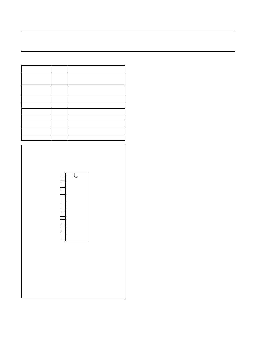
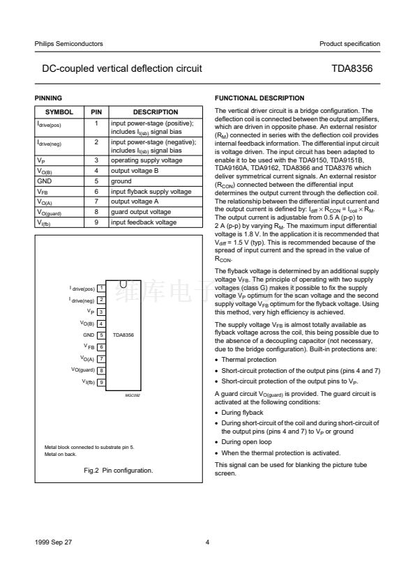
PINNING
SYMBOL
I
drive(pos)
I
drive(neg)
V
P
V
O(B)
GND
V
FB
V
O(A)
V
O(guard)
V
I(fb)
PIN
1
2
3
4
5
6
7
8
9
DESCRIPTION
input power-stage (positive);
includes I
I(sb)
signal bias
input power-stage (negative);
includes I
I(sb)
signal bias
operating supply voltage
output voltage B
ground
input 铿倅back supply voltage
output voltage A
guard output voltage
input feedback voltage
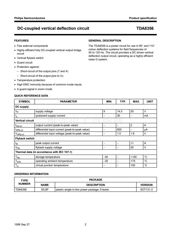
FUNCTIONAL DESCRIPTION
TDA8356
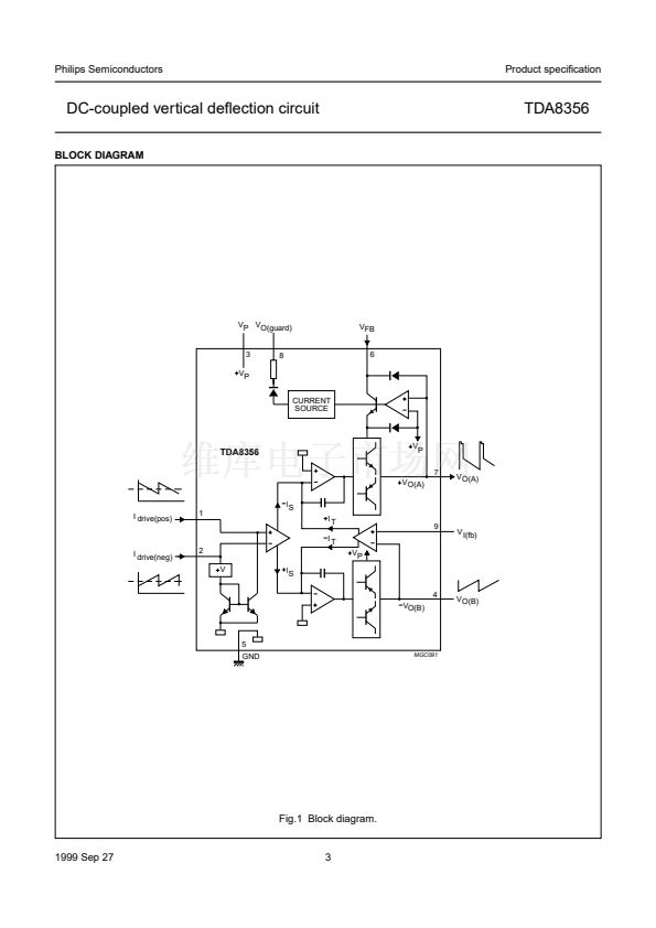
The vertical driver circuit is a bridge configuration. The
deflection coil is connected between the output amplifiers,
which are driven in opposite phase. An external resistor
(R
M
) connected in series with the deflection coil provides
internal feedback information. The differential input circuit
is voltage driven. The input circuit has been adapted to
enable it to be used with the TDA9150, TDA9151B,
TDA9160A, TDA9162, TDA8366 and TDA8376 which
deliver symmetrical current signals. An external resistor
(R
CON
) connected between the differential input
determines the output current through the deflection coil.
The relationship between the differential input current and
the output current is defined by: I
diff
脳
R
CON
= I
coil
脳
R
M
.
The output current is adjustable from 0.5 A (p-p) to
2 A (p-p) by varying R
M
. The maximum input differential
voltage is 1.8 V. In the application it is recommended that
V
diff
= 1.5 V (typ). This is recommended because of the
spread of input current and the spread in the value of
R
CON
.
The flyback voltage is determined by an additional supply
voltage V
FB
. The principle of operating with two supply
voltages (class G) makes it possible to fix the supply
voltage V
P
optimum for the scan voltage and the second
supply voltage V
FB
optimum for the flyback voltage. Using
this method, very high efficiency is achieved.
The supply voltage V
FB
is almost totally available as
flyback voltage across the coil, this being possible due to
the absence of a decoupling capacitor (not necessary,
due to the bridge configuration). Built-in protections are:
鈥?/div>
Thermal protection
鈥?/div>
Short-circuit protection of the output pins (pins 4 and 7)
鈥?/div>
Short-circuit protection of the output pins to V
P
.
A guard circuit V
O(guard)
is provided. The guard circuit is
activated at the following conditions:
鈥?/div>
During flyback
鈥?/div>
During short-circuit of the coil and during short-circuit of
the output pins (pins 4 and 7) to V
P
or ground
handbook, 2 columns
I drive(pos)
1
2
I drive(neg)
VP
VO(B)
GND
V FB
VO(A)
VO(guard)
V I(fb)
3
4
5
6
7
8
9
MGC092
TDA8356
Metal block connected to substrate pin 5.
Metal on back.
鈥?/div>
During open loop
鈥?/div>
When the thermal protection is activated.
This signal can be used for blanking the picture tube
screen.
Fig.2 Pin configuration.
1999 Sep 27
4
TDA8356 PDF文件相关型号
TDA8356
TDA8356相关型号PDF文件下载
-
型号
版本
描述
厂商
下载
-
英文版
Octuple 6-bit DACs with I2C-bus
PHILIPS
-
英文版
Octuple 6-bit DACs with I2C-bus
PHILIPS [N...
-
英文版
Smart card interface
PHILIPS
-
英文版
Smart card interface
PHILIPS [N...
-
英文版
Smart card interface
PHILIPS
-
英文版
Smart card interface
PHILIPS [N...
-
英文版
IC card interface
PHILIPS
-
英文版
IC card interface
PHILIPS [N...
-
英文版
IC card interface
PHILIPS
-
英文版
IC card interface
PHILIPS [N...
-
英文版
Low-power smart card coupler
PHILIPS
-
英文版
Low-power smart card coupler
PHILIPS [N...
-
英文版
Multiprotocol IC Card coupler
Philips
-
英文版
Dual multiprotocol smart card
Philips
-
英文版
Low power mixers/oscillators for satellite tuners
PHILIPS
-
英文版
Low power mixers/oscillators for satellite tuners
PHILIPS [N...
-
英文版
IF amplifier for satellite TV receivers
PHILIPS
-
英文版
IF amplifier for satellite TV receivers
PHILIPS [N...
-
英文版
Dual smart card interface
PHILIPS
-
英文版
Dual smart card interface
PHILIPS [N...


 1
1
 2
2
 3
3
 4
4
 5
5
 6
6
 7
7
 8
8
 9
9
 10
10
 11
11
 12
12
