鈥?/div>
a
(
k
+
1
LEAB
=
---------------------------
)
; LENAB
=
-----------------------------
-
-
a
avg
a
avg
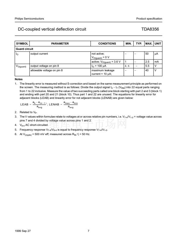
2. Related to V
P
.
3. The V values within formulae relate to voltages at or across relative pin numbers, i.e. V
7-4
/V
1-2
= voltage value across
pins 7 and 4 divided by voltage value across pins 1 and 2.
4. V
9-4
AC short-circuited.
5. Frequency response V
7-4
/V
9-4
is equal to frequency response V
7-4
/V
1-2
.
6. At V
(ripple)
= 500 mV eff; measured across R
M
; f
i
= 50 Hz.
1999 Sep 27
7


 1
1
 2
2
 3
3
 4
4
 5
5
 6
6
 7
7
 8
8
 9
9
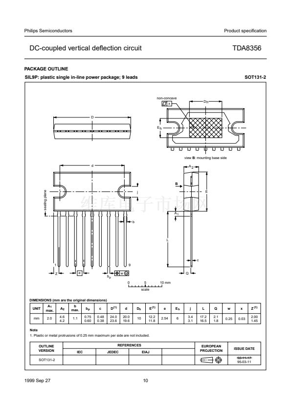 10
10
 11
11
 12
12
