TPS71501
TPS71525, TPS71530
TPS71533, TPS71550
SLVS338H 鈥?MAY 2001 鈥?REVISED JUNE 2004
www.ti.com
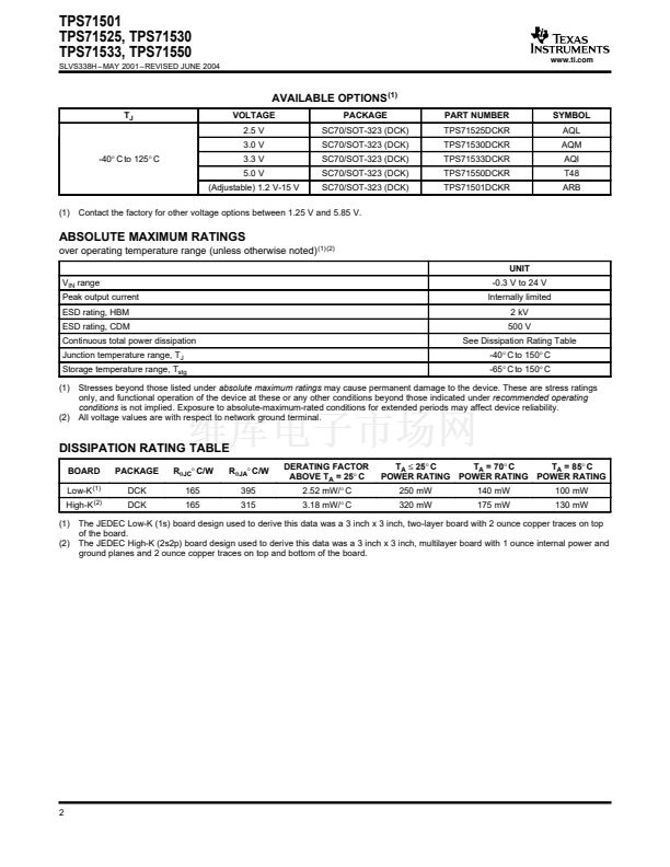
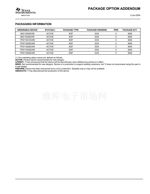
AVAILABLE OPTIONS
(1)
T
J
VOLTAGE
2.5 V
3.0 V
-40掳C to 125掳C
3.3 V
5.0 V
(Adjustable) 1.2 V-15 V
(1)
PACKAGE
SC70/SOT-323 (DCK)
SC70/SOT-323 (DCK)
SC70/SOT-323 (DCK)
SC70/SOT-323 (DCK)
SC70/SOT-323 (DCK)
PART NUMBER
TPS71525DCKR
TPS71530DCKR
TPS71533DCKR
TPS71550DCKR
TPS71501DCKR
SYMBOL
AQL
AQM
AQI
T48
ARB
Contact the factory for other voltage options between 1.25 V and 5.85 V.
ABSOLUTE MAXIMUM RATINGS
over operating temperature range (unless otherwise noted)
(1) (2)
UNIT
V
IN
range
Peak output current
ESD rating, HBM
ESD rating, CDM
Continuous total power dissipation
Junction temperature range, T
J
Storage temperature range, T
stg
(1)
(2)
-0.3 V to 24 V
Internally limited
2 kV
500 V
See Dissipation Rating Table
-40掳C to 150掳C
-65掳C to 150掳C
Stresses beyond those listed under
absolute maximum ratings
may cause permanent damage to the device. These are stress ratings
only, and functional operation of the device at these or any other conditions beyond those indicated under
recommended operating
conditions
is not implied. Exposure to absolute-maximum-rated conditions for extended periods may affect device reliability.
All voltage values are with respect to network ground terminal.
DISSIPATION RATING TABLE
BOARD
Low-K
(1)
High-K
(2)
(1)
(2)
PACKAGE
DCK
DCK
R
胃JC
掳C/W
165
165
R
胃JA
掳C/W
395
315
DERATING FACTOR
ABOVE T
A
= 25掳C
2.52 mW/掳C
3.18 mW/掳C
T
A
鈮?/div>
25掳C
POWER RATING
250 mW
320 mW
T
A
= 70掳C
POWER RATING
140 mW
175 mW
T
A
= 85掳C
POWER RATING
100 mW
130 mW
The JEDEC Low-K (1s) board design used to derive this data was a 3 inch x 3 inch, two-layer board with 2 ounce copper traces on top
of the board.
The JEDEC High-K (2s2p) board design used to derive this data was a 3 inch x 3 inch, multilayer board with 1 ounce internal power and
ground planes and 2 ounce copper traces on top and bottom of the board.
2


 1
1
 2
2
 3
3
 4
4
 5
5
 6
6
 7
7
 8
8
 9
9
 10
10
 11
11
