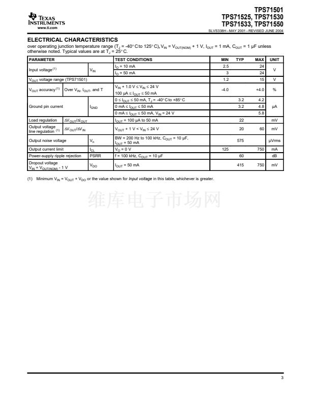
www.ti.com
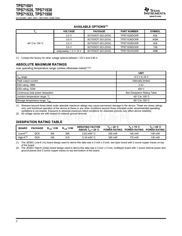
TPS71501
TPS71525, TPS71530
TPS71533, TPS71550
SLVS338H 鈥?MAY 2001 鈥?REVISED JUNE 2004
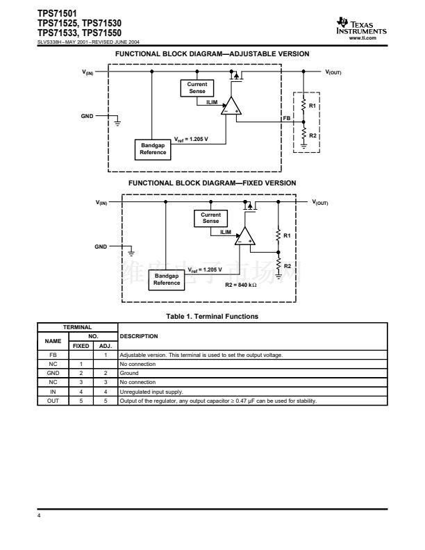
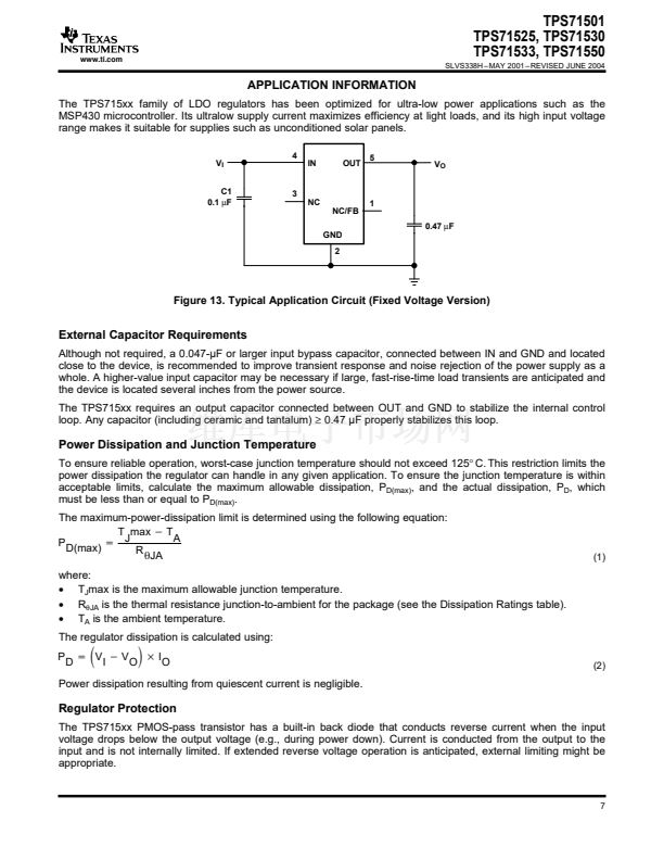
APPLICATION INFORMATION
The TPS715xx family of LDO regulators has been optimized for ultra-low power applications such as the
MSP430 microcontroller. Its ultralow supply current maximizes efficiency at light loads, and its high input voltage
range makes it suitable for supplies such as unconditioned solar panels.
V
I
C1
0.1
碌F
4
IN
OUT
5
V
O
3
NC
NC/FB
GND
2
0.47
碌F
1
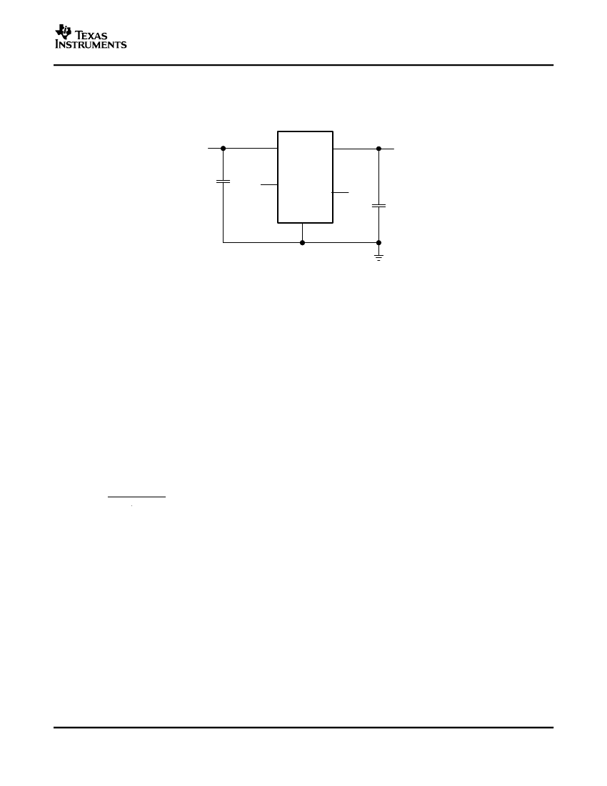
Figure 13. Typical Application Circuit (Fixed Voltage Version)
External Capacitor Requirements
Although not required, a 0.047-碌F or larger input bypass capacitor, connected between IN and GND and located
close to the device, is recommended to improve transient response and noise rejection of the power supply as a
whole. A higher-value input capacitor may be necessary if large, fast-rise-time load transients are anticipated and
the device is located several inches from the power source.
The TPS715xx requires an output capacitor connected between OUT and GND to stabilize the internal control
loop. Any capacitor (including ceramic and tantalum)
鈮?/div>
0.47 碌F properly stabilizes this loop.
Power Dissipation and Junction Temperature
To ensure reliable operation, worst-case junction temperature should not exceed 125掳C. This restriction limits the
power dissipation the regulator can handle in any given application. To ensure the junction temperature is within
acceptable limits, calculate the maximum allowable dissipation, P
D(max)
, and the actual dissipation, P
D
, which
must be less than or equal to P
D(max)
.
The maximum-power-dissipation limit is determined using the following equation:
T max
*
T
A
P
+
J
D(max)
R
qJA
where:
鈥?/div>
T
J
max is the maximum allowable junction temperature.
鈥?/div>
R
胃JA
is the thermal resistance junction-to-ambient for the package (see the Dissipation Ratings table).
鈥?/div>
T
A
is the ambient temperature.
The regulator dissipation is calculated using:
P
D
+
V
*
V
I
O
I
O
(2)
(1)
Power dissipation resulting from quiescent current is negligible.
Regulator Protection
The TPS715xx PMOS-pass transistor has a built-in back diode that conducts reverse current when the input
voltage drops below the output voltage (e.g., during power down). Current is conducted from the output to the
input and is not internally limited. If extended reverse voltage operation is anticipated, external limiting might be
appropriate.
7


 1
1
 2
2
 3
3
 4
4
 5
5
 6
6
 7
7
 8
8
 9
9
 10
10
 11
11
