TPS72615, TPS72616
TPS72618, TPS72625
SLVS403C 鈥?MAY 2002 鈥?REVISED MARCH 2004
www.ti.com
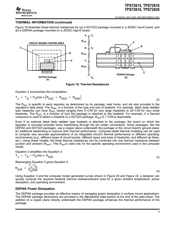
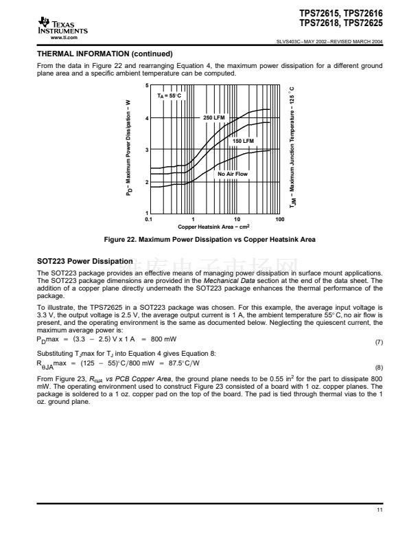
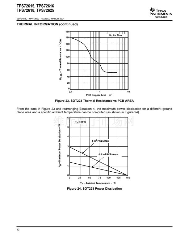
THERMAL INFORMATION (continued)
To illustrate, the TPS72625 in a DDPAK package was chosen. For this example, the average input voltage is 5
V, the output voltage is 2.5 V, the average output current is 1 A, the ambient temperature 55掳C, the air flow is
150 LFM, and the operating environment is the same as documented below. Neglecting the quiescent current,
the maximum average power is:
P
D
max
+
(5
*
2.5) V x 1 A
+
2.5 W
(5)
Substituting T
J
max for T
J
into Equation 4 gives Equation 6:
R
max
+
(125
*
55)掳C 2.5 W
+
28掳C W
胃JA
(6)
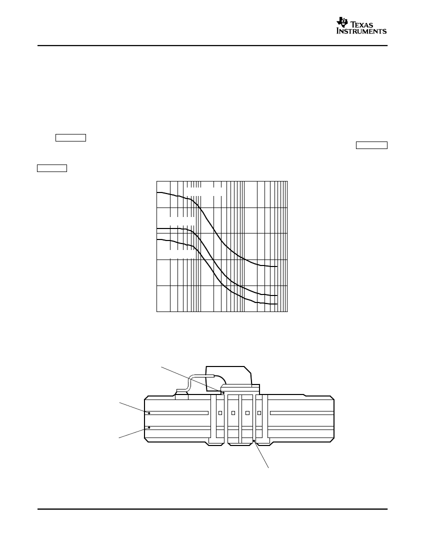
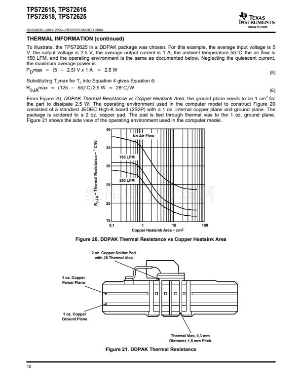
From Figure 20,
DDPAK Thermal Resistance vs Copper Heatsink Area,
the ground plane needs to be 1 cm
2
for
the part to dissipate 2.5 W. The operating environment used in the computer model to construct Figure 20
consisted of a standard JEDEC High-K board (2S2P) with a 1 oz. internal copper plane and ground plane. The
package is soldered to a 2 oz. copper pad. The pad is tied through thermal vias to the 1 oz. ground plane.
Figure 21 shows the side view of the operating environment used in the computer model.
40
No Air Flow
掳
C/W
R
胃
JA 鈭?Thermal Resistance 鈭?/div>
35
150 LFM
30
250 LFM
25
20
15
0.1
1
10
Copper Heatsink Area 鈭?cm
2
100
Figure 20. DDPAK Thermal Resistance vs Copper Heatsink Area
2 oz. Copper Solder Pad
with 25 Thermal Vias
1 oz. Copper
Power Plane
1 oz. Copper
Ground Plane
Thermal Vias, 0,3 mm
Diameter, 1,5 mm Pitch
Figure 21. DDPAK Thermal Resistance
10


 1
1
 2
2
 3
3
 4
4
 5
5
 6
6
 7
7
 8
8
 9
9
 10
10
 11
11
 12
12
 13
13
 14
14
 15
15
