TPS72615, TPS72616
TPS72618, TPS72625
SLVS403C 鈥?MAY 2002 鈥?REVISED MARCH 2004
www.ti.com
APPLICATION INFORMATION
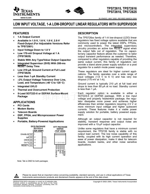
The TPS726xx family of low-dropout (LDO) regulators have numerous features that make it apply to a wide
range of applications. The family operates with very low input voltage (鈮?.8 V) and low dropout voltage (typically
200 mV at full load), making it an efficient stand-alone power supply or post regulator for battery or switch mode
power supplies. Both the active low RESET and 1-A output current, make the TPS726xx family ideal for
powering processor and FPGA supplies. The TPS726xx family also has low output noise (typically 150 碌V
RMS
with 10-碌F output capacitor), making it ideal for use in telecom equipment.
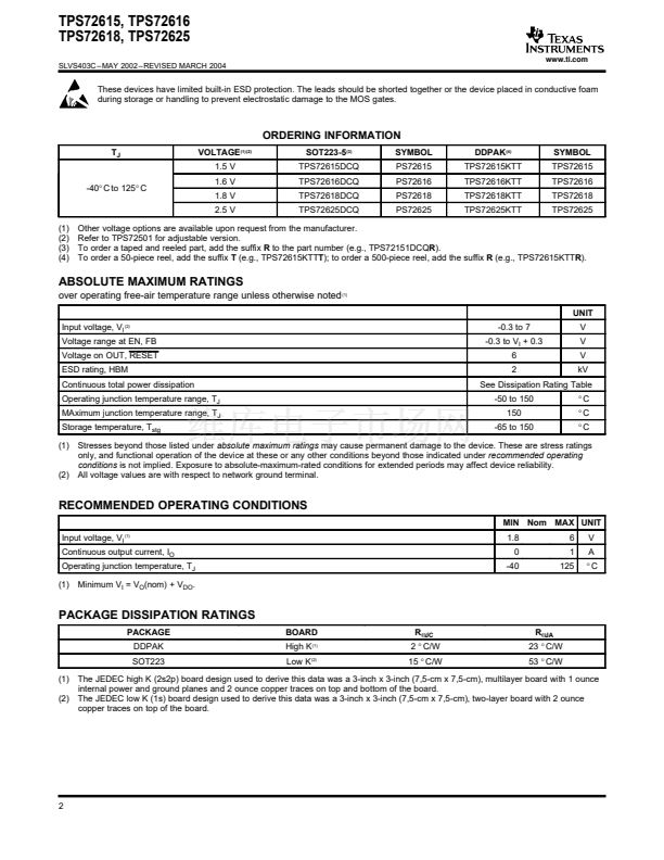
External Capacitor Requirements
A 1-碌F or larger ceramic input bypass capacitor, connected between IN and GND and located close to the
TPS725xx, is required for stability. To improve transient response, noise rejection, and ripple rejection, an
additional 10-碌F or larger, low ESR capacitor is recommended. A higher-value, low ESR input capacitor may be
necessary if large, fast-rise-time load transients are anticipated and the device is located several inches from the
power source, especially if the minimum input voltage of 1.8 V is used.
Although an output capacitor is not required for stability, transient response and output noise are improved with a
10-碌F output capacitor.
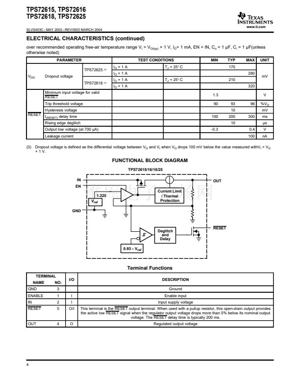
Regulator Protection
The TPS726xx pass element has a built-in back diode that safely conducts reverse current when the input
voltage drops below the output voltage (e.g., during power down). Current is conducted from the output to the
input and is not internally limited. If extended reverse voltage is anticipated, external limiting might be
appropriate.
The TPS726xx also features internal current limiting and thermal protection. During normal operation, the
TPS726xx limits output current to approximately 1.6 A. When current limiting engages, the output voltage scales
back linearly until the overcurrent condition ends. While current limiting is designed to prevent gross device
failure, care should be taken not to exceed the power dissipation ratings of the package. If the temperature of the
device exceeds 165掳C, thermal-protection circuitry shuts it down. Once the device has cooled down to below
145掳C, regulator operation resumes.
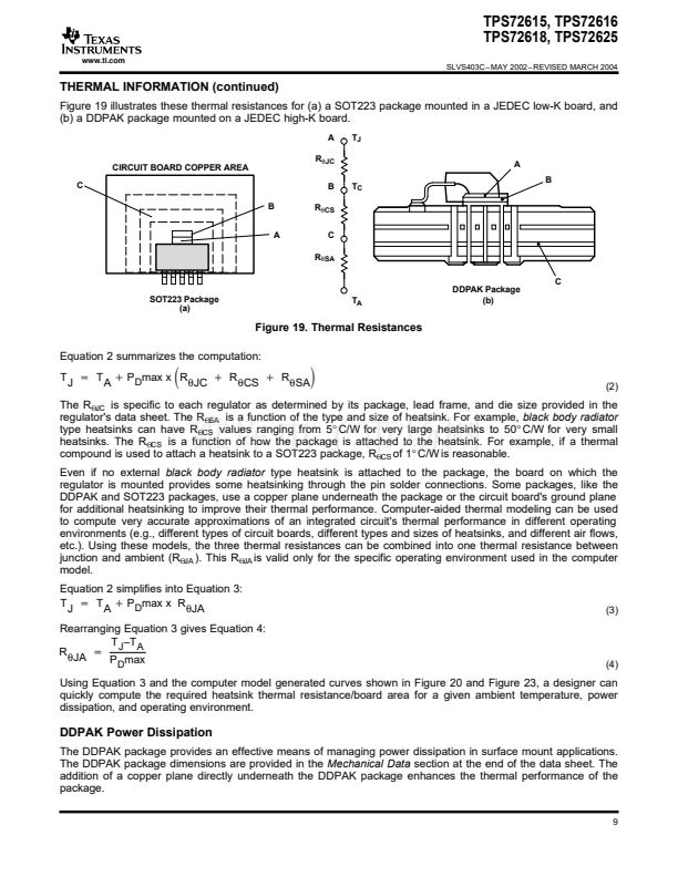
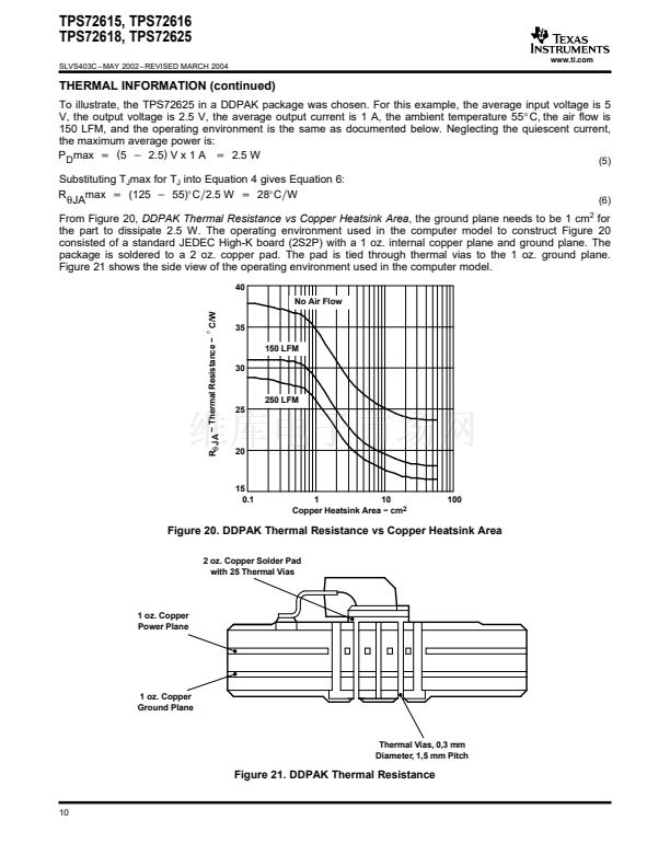
THERMAL INFORMATION
The amount of heat that an LDO linear regulator generates is directly proportional to the amount of power it
dissipates during operation. All integrated circuits have a maximum allowable junction temperature (T
J
max)
above which normal operation is not assured. A system designer must design the operating environment so that
the operating junction temperature (T
J
) does not exceed the maximum junction temperature (T
J
max). The two
main environmental variables that a designer can use to improve thermal performance are air flow and external
heatsinks. The purpose of this information is to aid the designer in determining the proper operating environment
for a linear regulator that is operating at a specific power level.
In general, the maximum expected power (P
D(max)
) consumed by a linear regulator is computed as:
P max
+
V
*
V
D
I(avg)
O(avg)
I
O(avg)
)
V
I(avg)
xI
(Q)
(1)
Where:
鈥?/div>
V
I(avg)
is the average input voltage.
鈥?/div>
V
O(avg)
is the average output voltage.
鈥?/div>
O(avg)
is the average output current.
鈥?/div>
I
(Q)
is the quiescent current.
For most TI LDO regulators, the quiescent current is insignificant compared to the average output current;
therefore, the term V
I(avg)
x I
(Q)
can be neglected. The operating junction temperature is computed by adding the
ambient temperature (T
A
) and the increase in temperature due to the regulator's power dissipation. The
temperature rise is computed by multiplying the maximum expected power dissipation by the sum of the thermal
resistances between the junction and the case (R
螛JC
), the case to heatsink (R
螛CS
), and the heatsink to ambient
(R
螛SA
). Thermal resistances are measures of how effectively an object dissipates heat. Typically, the larger the
device, the more surface area available for power dissipation and the lower the object's thermal resistance.
8


 1
1
 2
2
 3
3
 4
4
 5
5
 6
6
 7
7
 8
8
 9
9
 10
10
 11
11
 12
12
 13
13
 14
14
 15
15
