




LPC2939设计在MCU USB接口技术的应用
出处:幸福永远 发布于:2011-09-02 08:38:22
LPC2939以ARM968E-S CPU为内核,在一个芯片中集成了两个操作频率高达125MHz的TCM模块、全速USB2.0主机/OTG/设备控制器、CAN和LIN、56KB SRAM、768KB Flash存储器、外部存储器接口、3个10位ADC和多个串行、并行接口,定位于消费应用、工业、医疗、通信和汽车制造业市场。为了使系统功耗化,LPC2939具有一个非常灵活的时钟产生单元(CGU),可提供动态时钟门控和调节。本文介绍了LPC2939主要特性, 方框图,以及各种USB,USB OTG接口方框图。
MCU(MicroControlUnit)中文名称为微控制单元,又称单片微型计算机(SingleChipMicrocomputer)或者单片机,是指随着大规模集成电路的出现及其发展,将计算机的CPU、RAM、ROM、定时计数器和多种I/O接口集成在一片芯片上,形成芯片级的计算机,为不同的应用场合做不同组合控制。微控制器在经过这几年不断地研究,发展,历经4位,8位,到现在的16位及32位,甚至64位。产品的成熟度,以及投入厂商之多,应用范围之广,真可谓之空前。目前在国外大厂因开发较早,产品线广,所以技术,而本土厂商则以多功能为产品导向取胜。但不可讳言的,本土厂商的价格战是对外商造成威胁的关键因素
LPC2939: ARM9 microcontroller with CAN, LIN, and USB
The LPC2939 combine an ARM968E-S CPU core with two integrated TCM blocks operating at frequencies of up to 125 MHz, Full-speed USB 2.0 Host/OTG/Device controller, CAN and LIN, 56 kB SRAM, 768 kB flash memory, external memory interface,three 10-bit ADCs, and multiple serial and parallel interfaces in a single chip targeted at consumer, industrial, medical, and communication markets. To optimize system power
consumption, the LPC2939 has a very flexible Clock Generation Unit (CGU) that provides dynamic clock gating and scaling.
LPC2939主要特性和优势:
ARM968E-S processor running at frequencies of up to 125 MHz maximum.
Multilayer AHB system bus at 125 MHz with four separate layers.
On-chip memory:
Two Tightly Coupled Memories (TCM), 32 kB Instruction (ITCM), 32 kB Data TCM (DTCM)
Two separate internal Static RAM (SRAM) instances; 32 kB SRAM and 16 kB SRAM
8 kB ETB SRAM, also usable for code execution and data
768 kB high-speed flash program memory
16 kB true EEPROM, byte-erasable/programmable
Dual-master, eight-channel GPDMA controller on the AHB multilayer matrix which can be used with the SPI interfaces and the UARTs, as well as for memory-to-memory transfers including the TCM memories
External Static Memory Controller (SMC) with eight memory banks; up to 32-bit data bus; up to 24-bit address bus
Serial interfaces:
USB 2.0 full-speed Host/OTG/Device controller with dedicated DMA controller and on-chip device PHY
Two-channel CAN controller supporting FullCAN and extensive message filtering
Two LIN master controllers with full hardware support for LIN communication. The LIN interface can be configured as UART to provide two additional UART interfaces.
Two 550 UARTs with 16-byte Tx and Rx FIFO depths, DMA support, modem control, and RS-485/EIA-485 (9-bit) support
Three full-duplex Q-SPIs with four slave-select lines; 16 bits wide; 8 locations deep;Tx FIFO and Rx FIFO
Two I2C-bus interfaces
Other peripherals:
One 10-bit ADC with 5.0 V measurement range and eight input channels with conversion times as low as 2.44 ?s per channel
Two 10-bit ADCs, 8-channels each, with 3.3 V measurement range provide an additional 16 analog inputs with conversion times as low as 2.44 ?s per channel. Each channel provides a compare function to minimize interrupts.
Multiple trigger-start option for all ADCs: timer, PWM, other ADC, and external signal input
Four 32-bit timers each containing four capture-and-compare registers linked to I/Os
Four six-channel PWMs (Pulse-Width Modulators) with capture and trap functionality
Two dedicated 32-bit timers to schedule and synchronize PWM and ADC
Quadrature encoder interface that can monitor one external quadrature encoder
32-bit watchdog with timer change protection, running on safe clock
Up to 152 general-purpose I/O pins with programmable pull-up, pull-down, or bus keeper
Vectored Interrupt Controller (VIC) with 16 priority levels
Up to 22 level-sensitive external interrupt pins, including USB, CAN and LIN wake-up features
Configurable clock-out pin for driving external system clocks
Processor wake-up from power-down via external interrupt pins and CAN or LIN activity
Flexible Reset Generator Unit (RGU) able to control resets of inpidual modules
Flexible Clock-Generation Unit (CGU) able to control clock frequency of inpidual modules:
On-chip very low-power ring oscillator; fixed frequency of 0.4 MHz; always on to provide a Safe_Clock source for system monitoring
On-chip crystal oscillator with a recommended operating range from 10 MHz to 25 MHz. PLL input range 10 MHz to 25 MHz.
On-chip PLL allows CPU operation up to a maximum CPU rate of 125 MHz
Generation of up to 11 base clocks
Seven fractional piders
Second, dedicated CGU with its own PLL generates USB clocks and a configurable clock output
Highly configurable system Power Management Unit (PMU):
clock control of inpidual modules
allows minimization of system operating power consumption in any configuration
Standard ARM test and debug interface with real-time in-circuit emulator
Boundary-scan test supported
ETM/ETB debug functions with 8 kB of dedicated SRAM also accessible for application code and data storage
Dual power supply:
CPU operating voltage: 1.8 V ? 5 %
I/O operating voltage: 2.7 V to 3.6 V; inputs tolerant up to 5.5 V
208-pin LQFP package
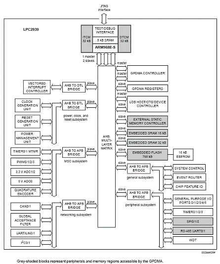
图1.LPC2939方框图
图2.LPC2939自供电设备USB接口方框图
图3.LPC2939总线供电设备USB接口方框图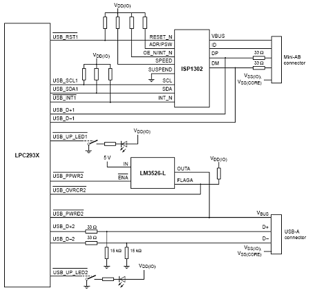
图4.LPC2939 USB OTG端口配置:USB端口1 OTG双任务设备,USB端口2主机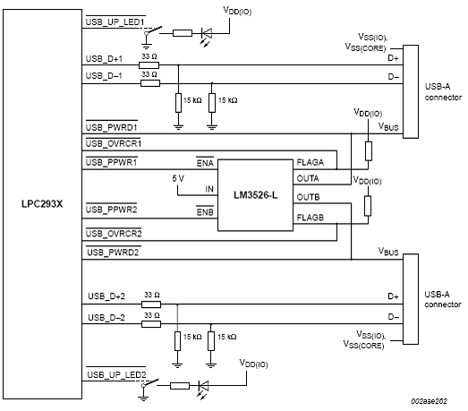
图5.LPC2939 USB OTG端口配置:USB端口1主机,USB端口2主机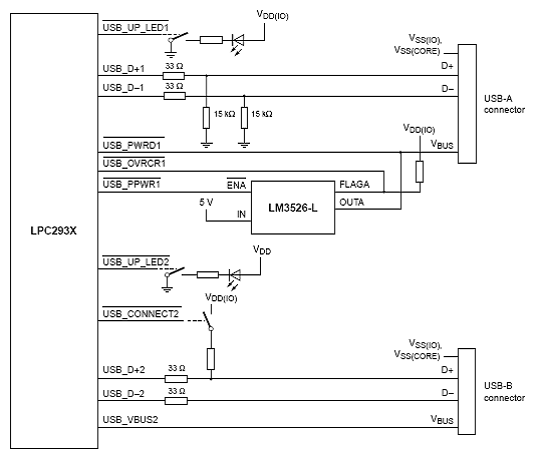
图6.LPC2939 USB OTG端口配置:USB端口2设备,USB端口1主机
版权与免责声明
凡本网注明“出处:维库电子市场网”的所有作品,版权均属于维库电子市场网,转载请必须注明维库电子市场网,https://www.dzsc.com,违反者本网将追究相关法律责任。
本网转载并注明自其它出处的作品,目的在于传递更多信息,并不代表本网赞同其观点或证实其内容的真实性,不承担此类作品侵权行为的直接责任及连带责任。其他媒体、网站或个人从本网转载时,必须保留本网注明的作品出处,并自负版权等法律责任。
如涉及作品内容、版权等问题,请在作品发表之日起一周内与本网联系,否则视为放弃相关权利。
- 你的嵌入式代码经常产生bug的五大原因2026/9/23 17:26:38
- 嵌入式模块化LCR测量解决方案在ATE系统中的应用案例2026/9/8 17:03:47
- 功率芯片 PCB 嵌入式封装技术综述2026/8/18 15:45:41
- Figma 到 GUI Guider 助力嵌入式 GUI 高效开发2026/8/13 15:30:50
- 瑞萨 RA8P1 嵌入式 AI 开发四部曲之零:工程挑战2026/8/12 16:03:16