128K X 36, 3.3V Synchronous
IDT71V547
SRAM with ZBT鈩?Feature, Burst
Counter and Flow-Through Outputs
Features
128K x 36 memory configuration, flow-through outputs
Supports high performance system speed - 95 MHz
(8ns Clock-to-Data Access)
ZBT
TM
Feature - No dead cycles between write and read
cycles
Internally synchronized signal eliminates the need to
control
OE
Single R/W (READ/WRITE) control pin
W
4-word burst capability (Interleaved or linear)
Individual byte write (BW
1
-
BW
4
) control (May tie active)
BW
Three chip enables for simple depth expansion
Single 3.3V power supply (卤5%)
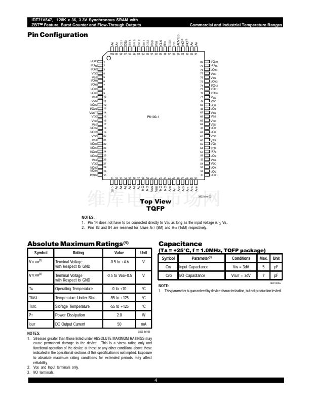
Packaged in a JEDEC standard 100-pin TQFP package
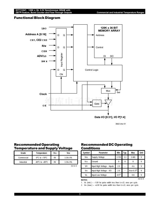
The IDT71V547 contains address, data-in and control signal registers.
The outputs are flow-through (no output data register). Output enable is
the only asynchronous signal and can be used to disable the outputs at
any given time.
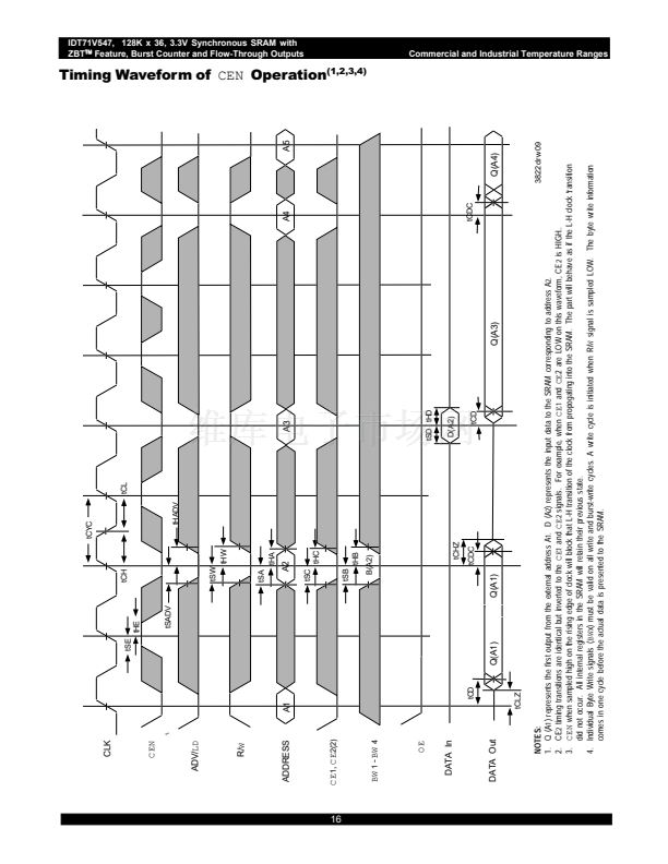
A Clock Enable (CEN) pin allows operation of the IDT71V547 to
be suspended as long as necessary. All synchronous inputs are
ignored when
CEN
is high and the internal device registers will hold
their previous values.
There are three chip enable pins (CE
1
, CE
2
,
CE
2
) that allow the user
to deselect the device when desired. If any one of these three is not active
when ADV/LD is low, no new memory operation can be initiated and any
burst in progress is stopped. However, any pending data transfers (reads
or writes) will be completed. The data bus will tri-state one cycle after the
chip was deselected or write initiated.
The IDT71V547 has an on-chip burst counter. In the burst mode, the
IDT71V547 can provide four cycles of data for a single address presented
to the SRAM. The order of the burst sequence is defined by the
LBO
input
pin. The
LBO
pin selects between linear and interleaved burst sequence.
The ADV/LD signal is used to load a new external address (ADV/LD =
LOW) or increment the internal burst counter (ADV/LD = HIGH).
The IDT71V547 SRAM utilizes IDT's high-performance, high-volume
3.3V CMOS process, and is packaged in a JEDEC Standard 14mm x
20mm 100-pin thin plastic quad flatpack (TQFP) for high board density.
x
x
x
x
x
x
x
x
x
x
Description
The IDT71V547 is a 3.3V high-speed 4,718,592-bit (4.5 Megabit)
synchronous SRAM organized as 128K x 36 bits. It is designed to eliminate
dead bus cycles when turning the bus around between reads and writes,
or writes and reads. Thus it has been given the name ZBT
TM
, or Zero Bus
Turn-around.
Address and control signals are applied to the SRAM during one clock
cycle, and on the next clock cycle, its associated data cycle occurs, be it
read or write.
Pin Description Summary
A
0
- A
16
CE
1
, CE
2
,
CE
2
OE
R/W
CEN
BW
1
,
BW
2
,
BW
3
,
BW
4
CLK
ADV/LD
LBO
I/O
0
- I/O
31
, I/O
P1
-
I/O
P4
V
DD
V
SS
Address Inputs
Three Chip Enables
Output Enable
Read/Write Signal
Clock Enable
Individual Byte Write Selects
Clock
Advance Burst Address / Load New Address
Linear / Interleaved Burst Order
Data Input/Output
3.3V Power
Ground
Input
Input
Input
Input
Input
Input
Input
Input
Input
I/O
Supply
Supply
Synchronous
Synchronous
Asynchronous
Synchronous
Synchronous
Synchronous
N/A
Synchronous
Static
Synchronous
Static
Static
3822 tbl 01
ZBT and Zero Bus Turnaround are trademarks of Integrated Device Technology, Inc. and the architecture is supported by Micron Technology and Motorola Inc.
DECEMBER 1999
DSC-3822/03
1
漏1999 Integrated Device Technology, Inc.


 1
1
 2
2
 3
3
 4
4
 5
5
 6
6
 7
7
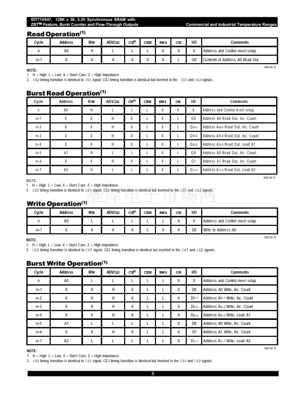 8
8
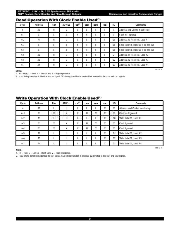 9
9
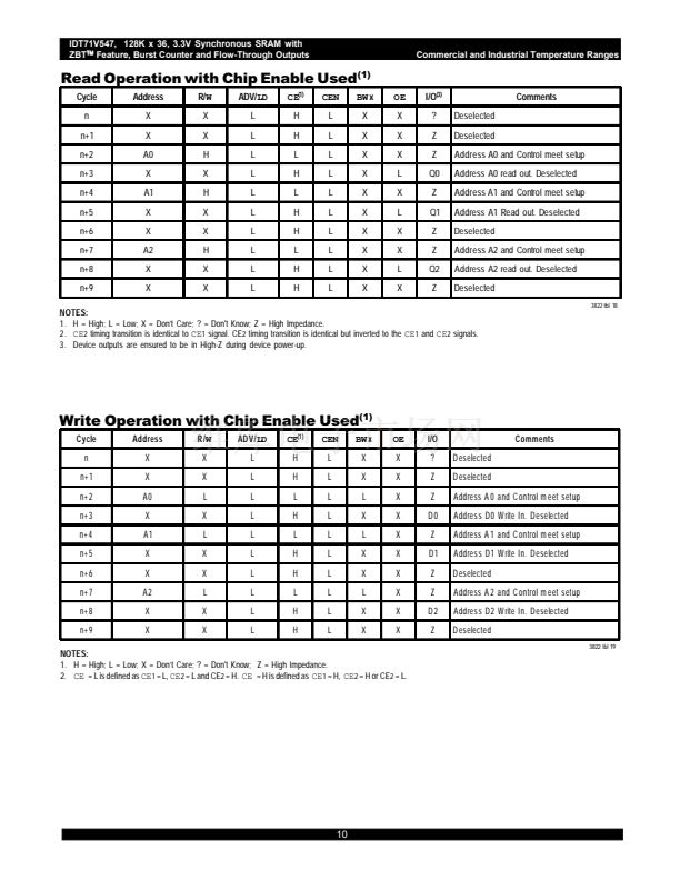 10
10
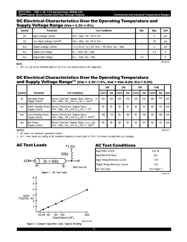 11
11
 12
12
 13
13
 14
14
 15
15
 16
16
 17
17
 18
18
 19
19
