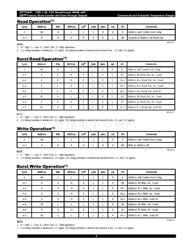
鈩?/div>
A1
A2
A3
A4
A5
A7
A8
A9
CE
1
,
CE
2
(2)
tSB
tHB
B(A2)
B(A4)
B(A5)
B(A8)
Timing Waveform of Combined Read and Write Cycles
(1,2,3)
15
6.42
tSD tHD
D(A2)
D(A4)
D(A5)
BW
1
-
BW
4
OE
D(A8)
DATA In
Write
tCHZ
tCLZ
tCDC
Write
Write
Write
tCD
DATA Out
Q(A1)
Read
Q(A3)
Q(A6)
Read
Q(A7)
Read
Read
Commercial and Industrial Temperature Ranges
3822 drw 08
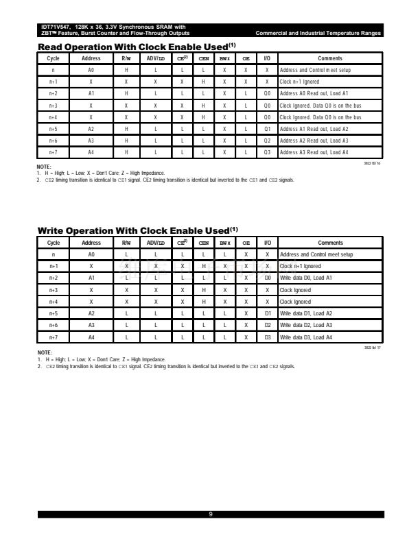
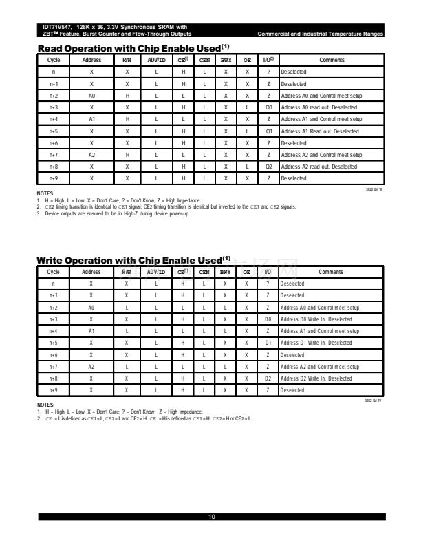
NOTES:
1. Q (A
1
) represents the first output from the external address A
1
. D (A
2
) represents the input data to the SRAM corresponding to address A
2
.
2. CE
2
timing transitions are identical but inverted to the
CE
1
and
CE
2
signals. For example, when
CE
1
and
CE
2
are LOW on this waveform, CE
2
is HIGH.
3. Individual Byte Write signals (BWx) must be valid on all write and burst-write cycles. A write cycle is initiated when R/W signal is sampled LOW. The byte write information
comes in one cycle before the actual data is presented to the SRAM.
,


 1
1
 2
2
 3
3
 4
4
 5
5
 6
6
 7
7
 8
8
 9
9
 10
10
 11
11
 12
12
 13
13
 14
14
 15
15
 16
16
 17
17
 18
18
 19
19
