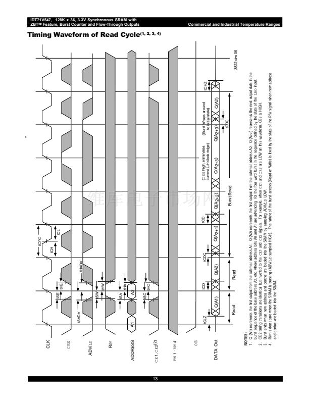
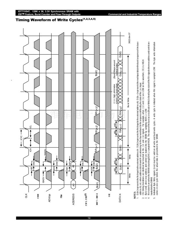
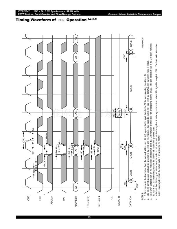
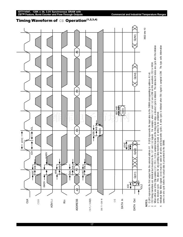
鈩?/div>
Commercial and Industrial Temperature Ranges
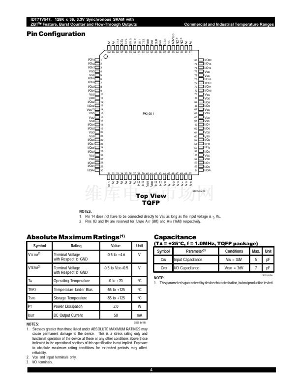
100 99 98 97 96 95 94 93 92 91 90 89 88 87 86 85 84 83 82 81
I/O
P3
I/O
16
I/O
17
V
DD
V
SS
I/O
18
I/O
19
I/O
20
I/O
21
V
SS
V
DD
I/O
22
I/O
23
V
SS
(1)
V
DD
V
DD
V
SS
I/O
24
I/O
25
V
DD
V
SS
I/O
26
I/O
27
I/O
28
I/O
29
V
SS
V
DD
I/O
30
I/O
31
I/O
P4
BW
2
BW
1
CE
2
V
DD
V
SS
CLK
R/W
C EN
OE
ADV/LD
NC
(2)
NC
(2)
A
8
A
9
Pin Configuration
A
6
A
7
CE
1
CE
2
BW
4
BW
3
1
2
3
4
5
6
7
8
9
10
11
12
13
14
15
16
17
18
19
20
21
22
23
24
25
26
27
28
29
30
31 32 33 34 35 36 37 38 39 40 41 42 43 44 45 46 47 48 49 50
80
79
78
77
76
75
74
73
72
71
70
69
68
67
PK100-1
66
65
64
63
62
61
60
59
58
57
56
55
54
53
52
51
I/O
P2
I/O
15
I/O
14
V
DD
V
SS
I/O
13
I/O
12
I/O
11
I/O
10
V
SS
V
DD
I/O
9
I/O
8
V
SS
V
SS
V
DD
V
SS
I/O
7
I/O
6
V
DD
V
SS
I/O
5
I/O
4
I/O
3
I/O
2
V
SS
V
DD
I/O
1
I/O
0
I/O
P1
LBO
A
5
A
4
A
3
A
2
A
1
A
0
NC
NC
V
SS
V
DD
NC
NC
A
10
A
11
A
12
A
13
A
14
A
15
A
16
Top View
TQFP
3822 drw 02
NOTES:
1. Pin 14 does not have to be connected directly to V
SS
as long as the input voltage is < V
IL
.
2. Pins 83 and 84 are reserved for future A
17
(8M) and A
18
(16M) respectively.
Absolute Maximum Ratings
(1)
Symbol
V
TERM
(2)
Rating
Terminal Voltage
with Respect to GND
Terminal Voltage
with Respect to GND
Operating Temperature
Temperature Under Bias
Storage Temperature
Power Dissipation
DC Output Current
Value
-0.5 to +4.6
-0.5 to V
DD
+0.5
0 to +70
-55 to +125
-55 to +125
2.0
50
Unit
V
V
o
(T
A
= +25掳C, f = 1.0MHz, TQFP package)
Symbol
C
IN
C
I/O
Parameter
(1)
Input Capacitance
I/O Capacitance
Conditions
V
IN
= 3dV
V
OUT
= 3dV
Max.
5
7
Unit
pF
pF
3822 tbl 06
Capacitance
V
TERM
(3)
T
A
T
BIAS
T
STG
P
T
I
OUT
C
C
C
NOTE:
1. This parameter is guaranteed by device characterization, but not production tested.
o
o
W
mA
3822 tbl 05
NOTES:
1. Stresses greater than those listed under ABSOLUTE MAXIMUM RATINGS may
cause permanent damage to the device. This is a stress rating only and
functional operation of the device at these or any other conditions above those
indicated in the operational sections of this specification is not implied. Exposure
to absolute maximum rating conditions for extended periods may affect
reliability.
2. V
DD
and Input terminals only.
3. I/O terminals.
4


 1
1
 2
2
 3
3
 4
4
 5
5
 6
6
 7
7
 8
8
 9
9
 10
10
 11
11
 12
12
 13
13
 14
14
 15
15
 16
16
 17
17
 18
18
 19
19
