SMBT3904PN
NPN/PNP Silicon Switching Transistor Array
High current gain
Low collector-emitter saturation voltage
Two (galvanic) internal isolated NPN/PNP
Transistors in one package
4
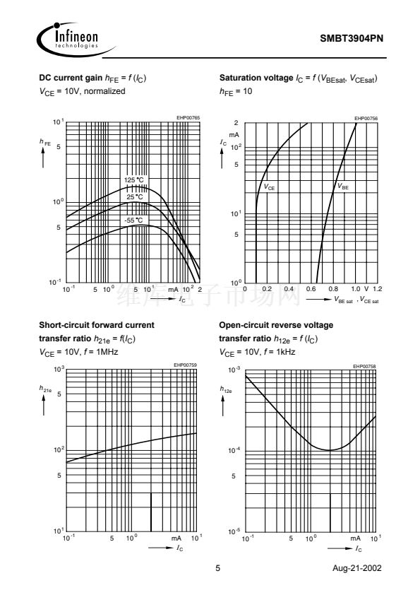
5
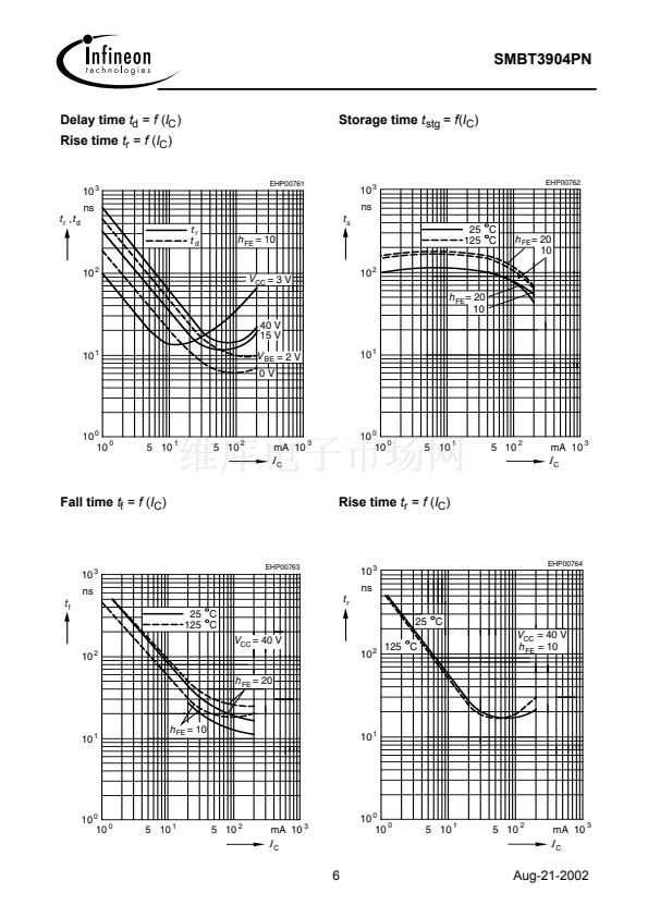
6
1For calculation of
R
thJA
please refer to Application Note Thermal Resistance
1
�
�
�
�
2
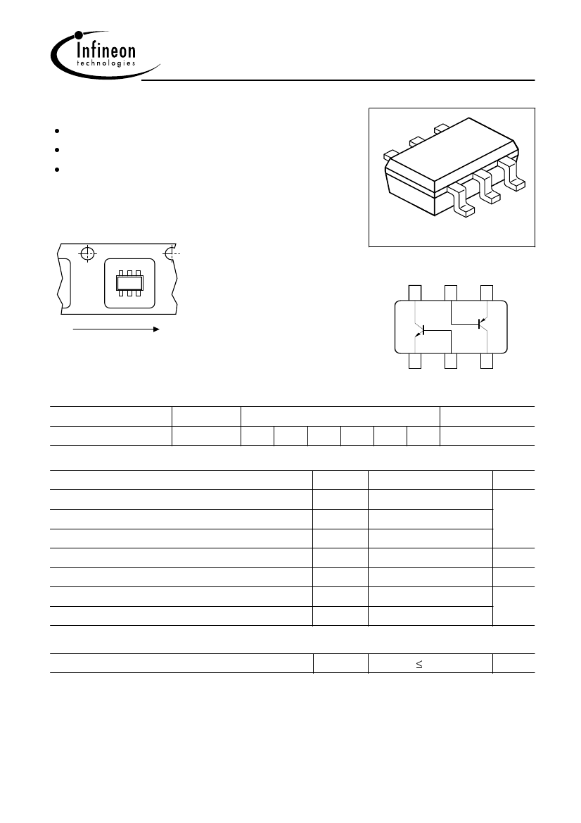
Tape loading orientation
Top View
6 5 4
W1s
1 2 3
Direction of Unreeling
Position in tape: pin 1
opposite of feed hole side
EHA07193
3
1
VPS05604
Marking on SOT-363 package
(for example W1s)
corresponds to pin 1 of device
C1
6
B2
5
E2
4
TR2
TR1
1
E1
2
B1
3
C2
EHA07177
Type
SMBT3904PN
Maximum Ratings
Parameter
Marking
s3P
Pin Configuration
Package
1 = E 2 = B 3 = C 4 = E 5 = B 6 = C SOT363
Symbol
V
CEO
V
CBO
V
EBO
I
C
P
tot
T
j
T
stg
Value
40
40
5
200
250
150
-65 ... 150
mA
mW
掳C
Unit
V
Collector-emitter voltage
Collector-base voltage
Emitter-base voltage
DC collector current
Total power dissipation,
T
S
= 115 掳C
Junction temperature
Storage temperature
Thermal Resistance
Thermal resistance, chip case
1)
R
thJC
140
K/W
Aug-21-2002


 1
1
 2
2
 3
3
 4
4
 5
5
 6
6
 7
7
