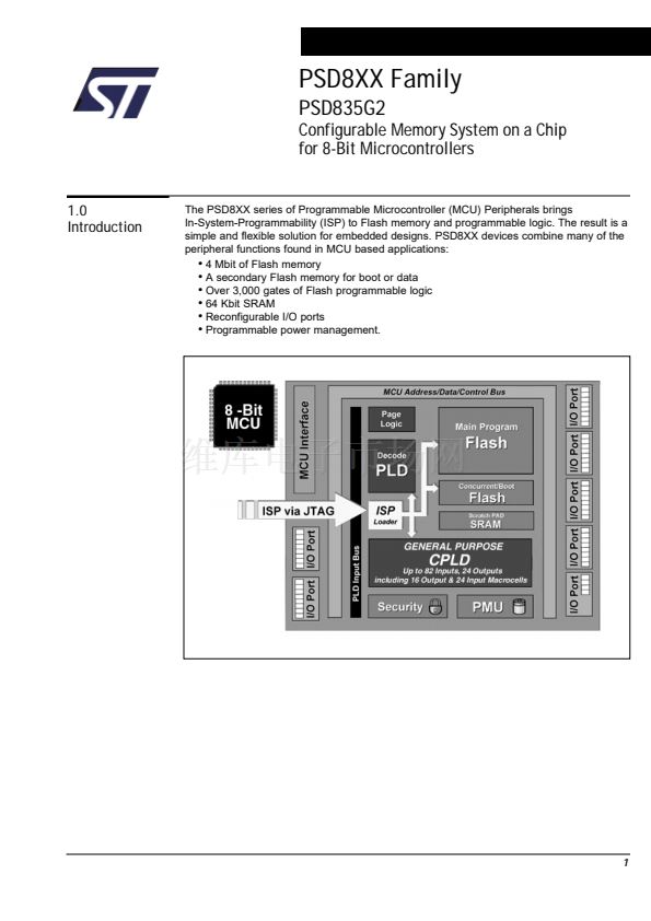
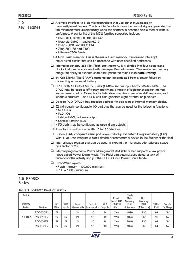
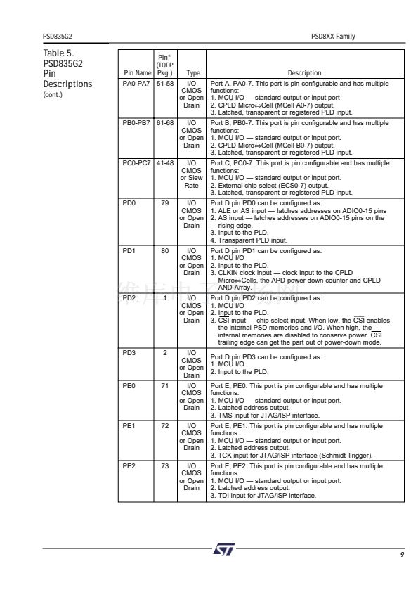
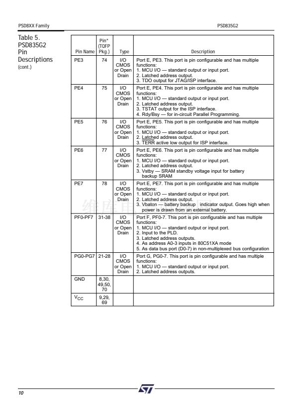
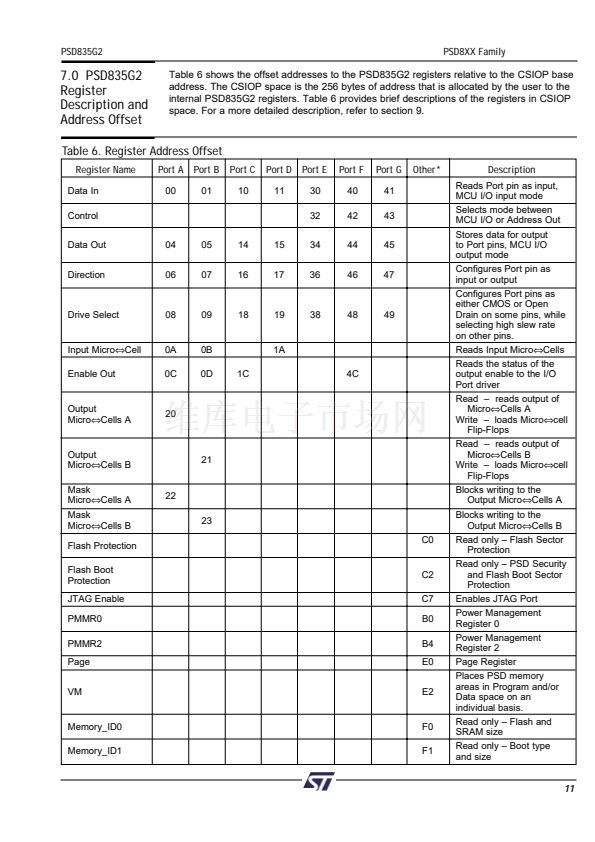
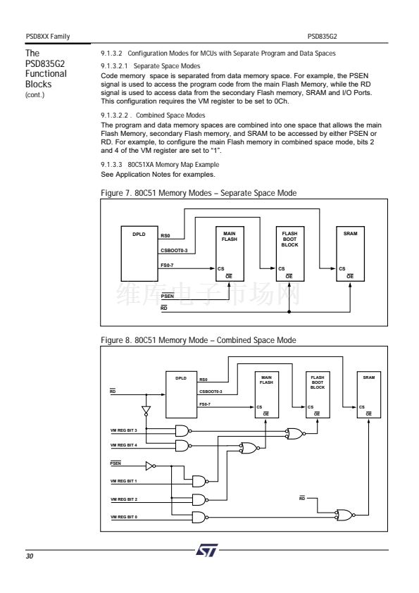
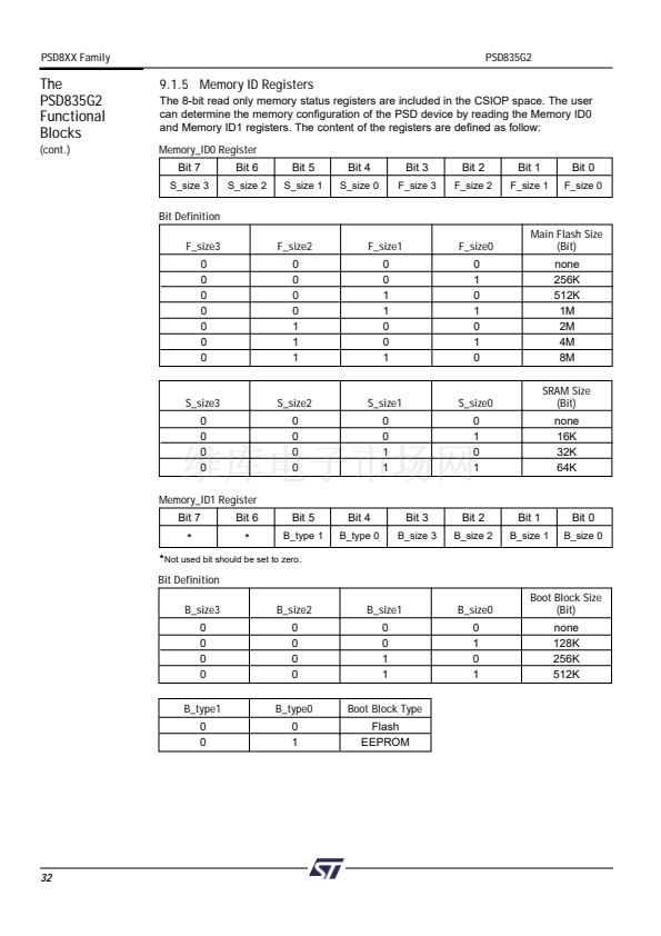
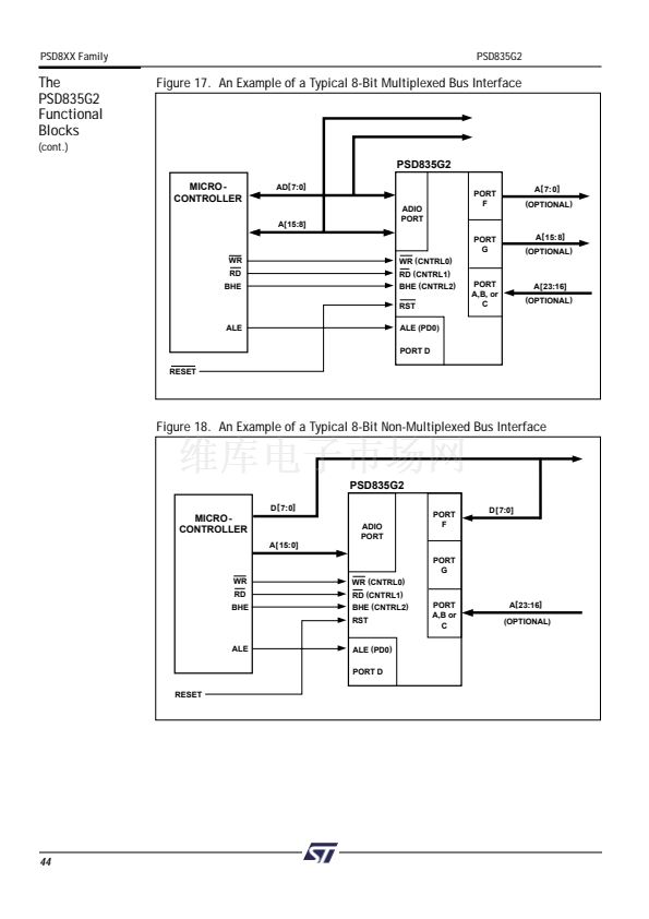
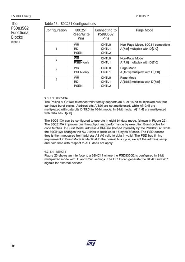
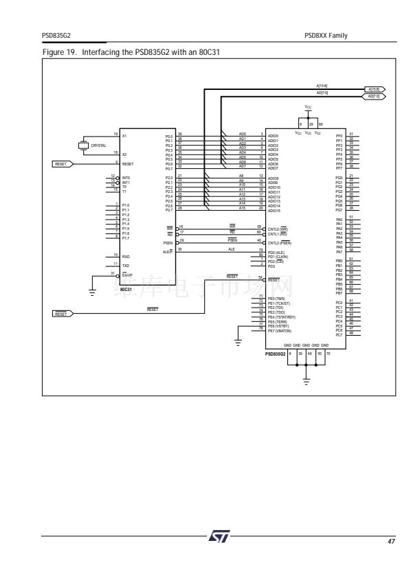
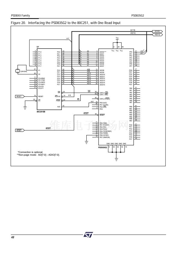
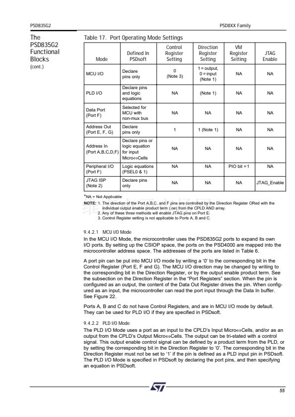
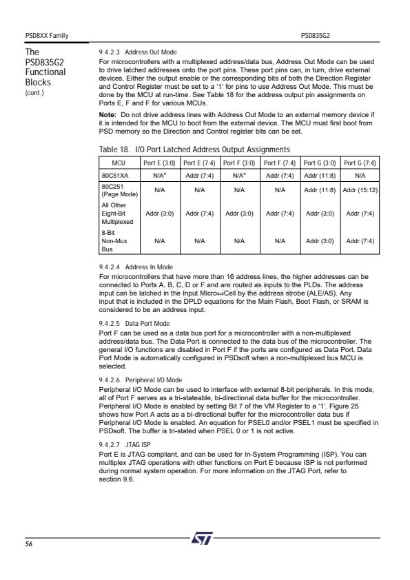
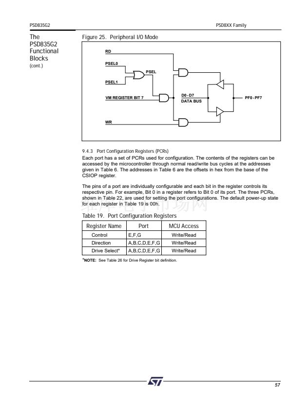
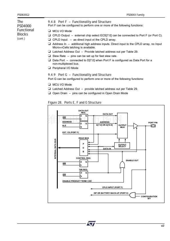
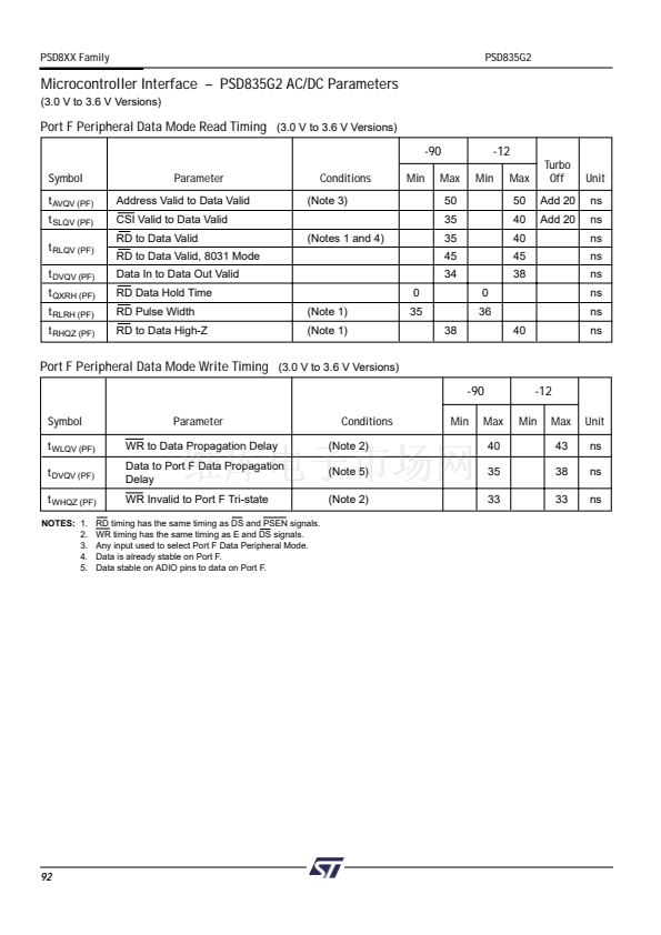
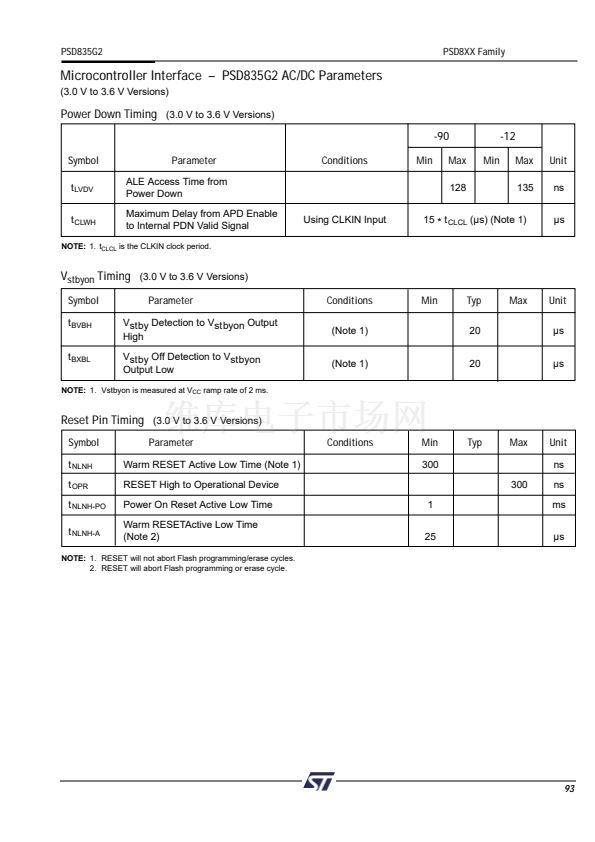
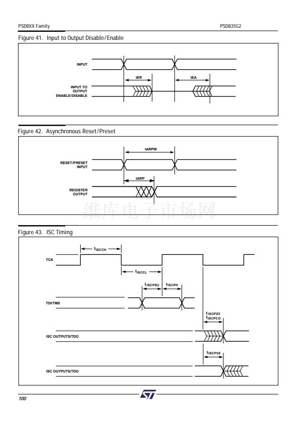
PSD8XX Family
PSD835G2
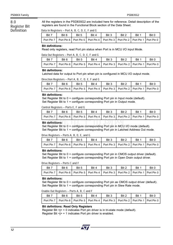
All the registers in the PSD835G2 are included here for reference. Detail description of the
registers are found in the Functional Block section of the Data Sheet.
Data In Registers 鈥?Port A, B, C, D, E, F and G
Bit 7
Port Pin 7
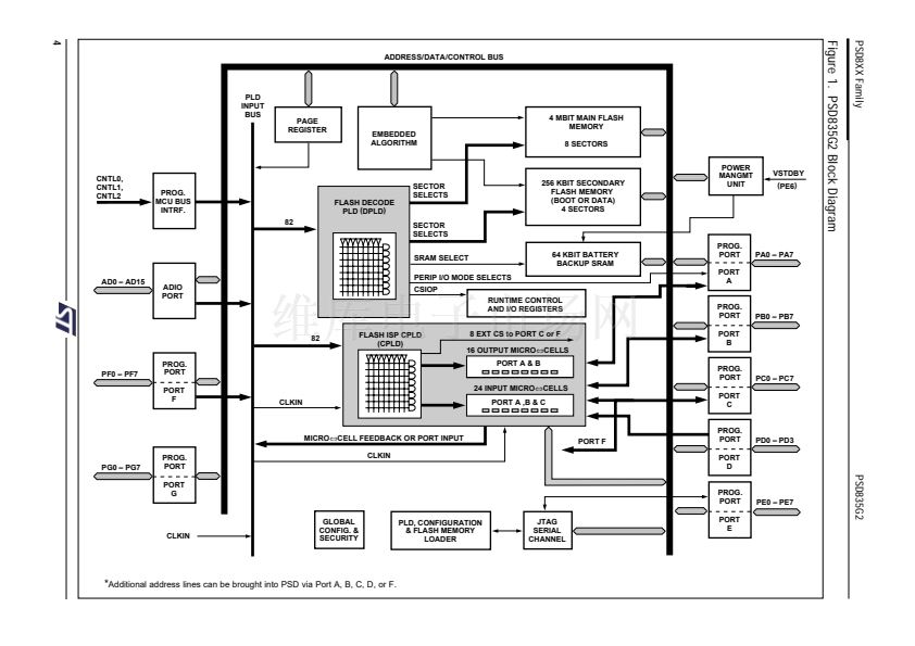
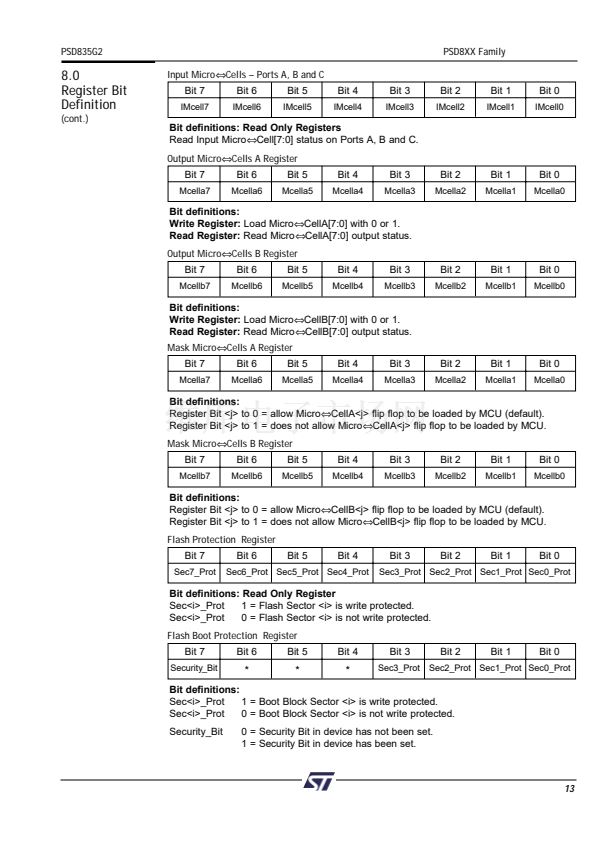
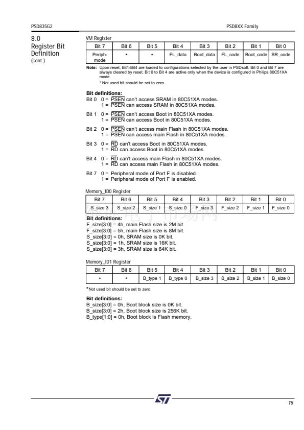
8.0
Register Bit
Definition
Bit 6
Port Pin 6
Bit 5
Port Pin 5
Bit 4
Port Pin 4
Bit 3
Port Pin 3
Bit 2
Port Pin 2
Bit 1
Bit 0
Port Pin 1 Port Pin 0
Bit definitions:
Read only registers, read Port pin status when Port is in MCU I/O input Mode.
Data Out Registers 鈥?Port A, B, C, D, E, F and G
Bit 7
Port Pin 7
Bit 6
Port Pin 6
Bit 5
Port Pin 5
Bit 4
Port Pin 4
Bit 3
Port Pin 3
Bit 2
Port Pin 2
Bit 1
Bit 0
Port Pin 1 Port Pin 0
Bit definitions:
Latched data for output to Port pin when pin is configured in MCU I/O output mode.
Direction Registers 鈥?Port A, B, C, D, E, F and G
Bit 7
Port Pin 7
Bit 6
Port Pin 6
Bit 5
Port Pin 5
Bit 4
Port Pin 4
Bit 3
Port Pin 3
Bit 2
Port Pin 2
Bit 1
Bit 0
Port Pin 1 Port Pin 0
Bit definitions:
Set Register Bit to 0 = configure corresponding Port pin in Input mode (default).
Set Register Bit to 1 = configure corresponding Port pin in Output mode.
Control Registers 鈥?Ports E, F and G
Bit 7
Port Pin 7
Bit 6
Port Pin 6
Bit 5
Port Pin 5
Bit 4
Port Pin 4
Bit 3
Port Pin 3
Bit 2
Port Pin 2
Bit 1
Bit 0
Port Pin 1 Port Pin 0
Bit definitions:
Set Register Bit to 0 = configure corresponding Port pin in MCU I/O mode (default).
Set Register Bit to 1 = configure corresponding Port pin in Latched Address Out mode.
Drive Registers 鈥?Ports A, B, D, E, and G
Bit 7
Port Pin 7
Bit 6
Port Pin 6
Bit 5
Port Pin 5
Bit 4
Port Pin 4
Bit 3
Port Pin 3
Bit 2
Port Pin 2
Bit 1
Bit 0
Port Pin 1 Port Pin 0
Bit definitions:
Set Register Bit to 0 = configure corresponding Port pin in CMOS output driver (default).
Set Register Bit to 1 = configure corresponding Port pin in Open Drain output driver.
Drive Registers 鈥?Ports C and F
Bit 7
Port Pin 7
Bit 6
Port Pin 6
Bit 5
Port Pin 5
Bit 4
Port Pin 4
Bit 3
Port Pin 3
Bit 2
Port Pin 2
Bit 1
Bit 0
Port Pin 1 Port Pin 0
Bit definitions:
Set Register Bit to 0 = configure corresponding Port pin as CMOS output driver (default).
Set Register Bit to 1 = configure corresponding Port pin in Slew Rate mode.
Enable Out Registers 鈥?Ports A, B, C and F
Bit 7
Port Pin 7
Bit 6
Port Pin 6
Bit 5
Port Pin 5
Bit 4
Port Pin 4
Bit 3
Port Pin 3
Bit 2
Port Pin 2
Bit 1
Bit 0
Port Pin 1 Port Pin 0
Bit definitions: Read Only Registers
Register Bit <j> = 0 indicates Port pin driver is in tri-state mode (default).
Register Bit <j> = 1 indicates Port pin driver is enabled.
12


 1
1
 2
2
 3
3
 4
4
 5
5
 6
6
 7
7
 8
8
 9
9
 10
10
 11
11
 12
12
 13
13
 14
14
 15
15
 16
16
 17
17
 18
18
 19
19
 20
20
 21
21
 22
22
 23
23
 24
24
 25
25
 26
26
 27
27
 28
28
 29
29
 30
30
 31
31
 32
32
 33
33
 34
34
 35
35
 36
36
 37
37
 38
38
 39
39
 40
40
 41
41
 42
42
 43
43
 44
44
 45
45
 46
46
 47
47
 48
48
 49
49
 50
50
 51
51
 52
52
 53
53
 54
54
 55
55
 56
56
 57
57
 58
58
 59
59
 60
60
 61
61
 62
62
 63
63
 64
64
 65
65
 66
66
 67
67
 68
68
 69
69
 70
70
 71
71
 72
72
 73
73
 74
74
 75
75
 76
76
 77
77
 78
78
 79
79
 80
80
 81
81
 82
82
 83
83
 84
84
 85
85
 86
86
 87
87
 88
88
 89
89
 90
90
 91
91
 92
92
 93
93
 94
94
 95
95
 96
96
 97
97
 98
98
 99
99
 100
100
 101
101
 102
102
 103
103
 104
104
 105
105
 106
106
 107
107
 108
108
 109
109
 110
110
