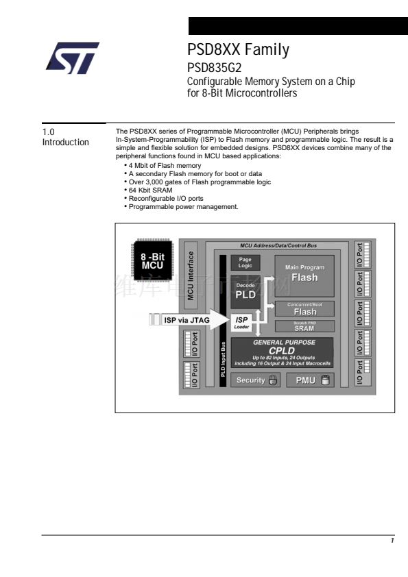
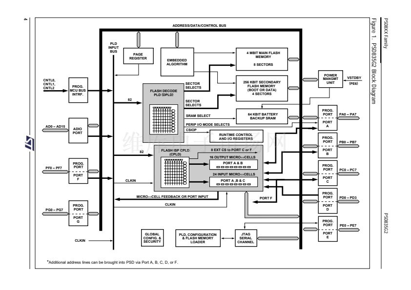
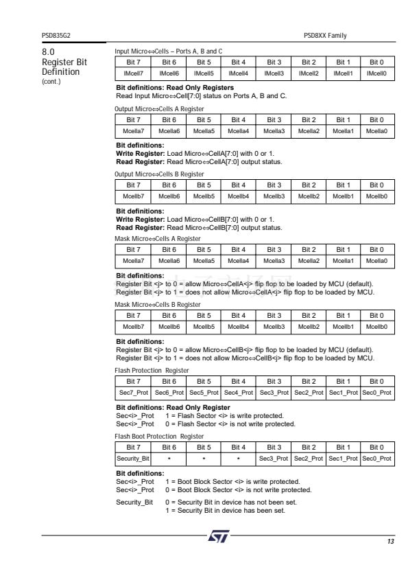
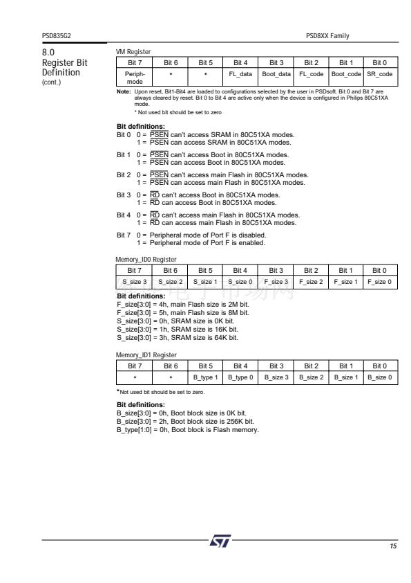
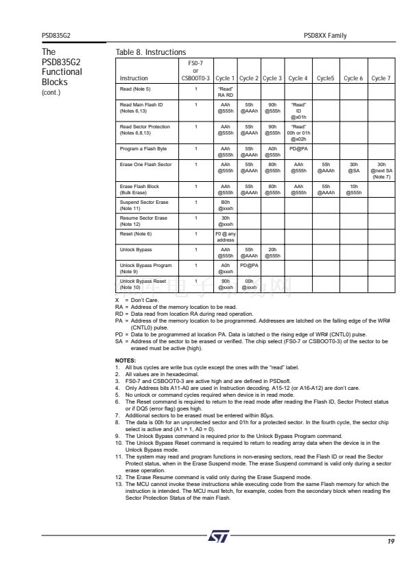
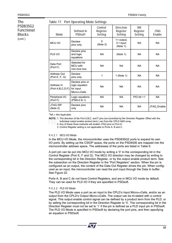
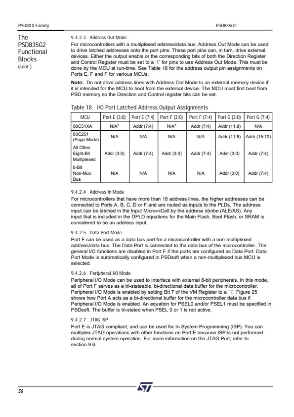
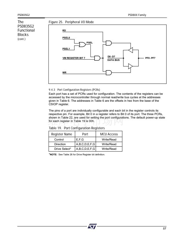
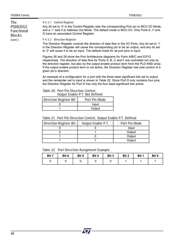
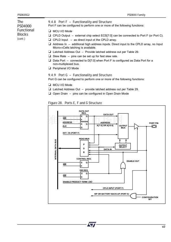
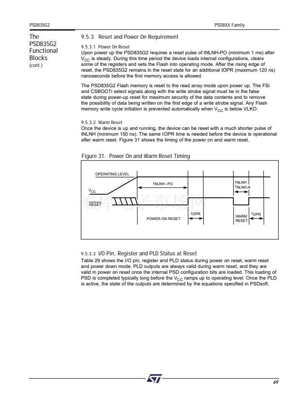
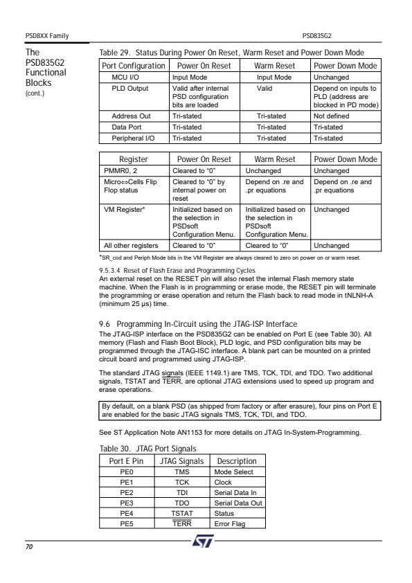
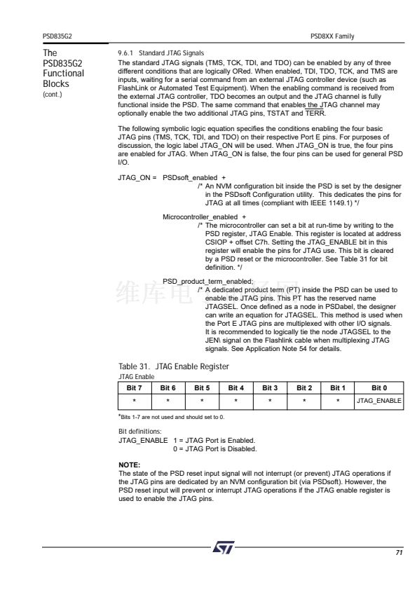
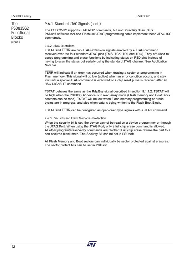
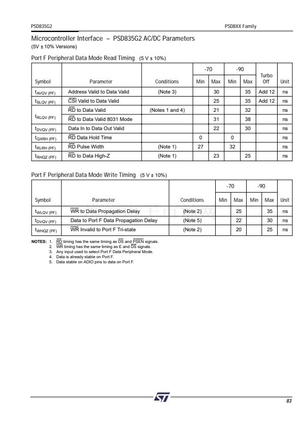
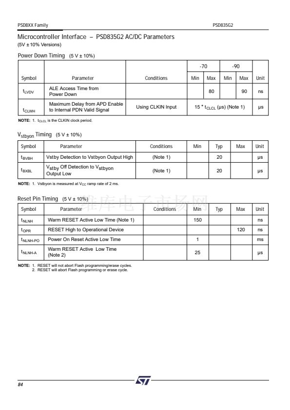
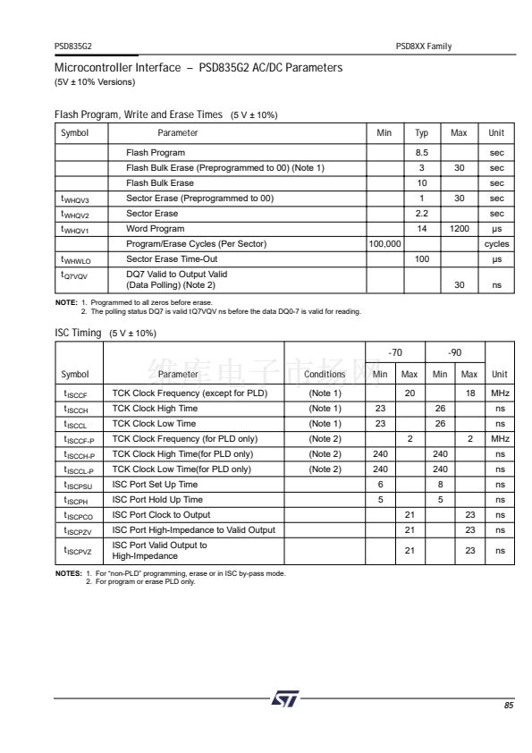
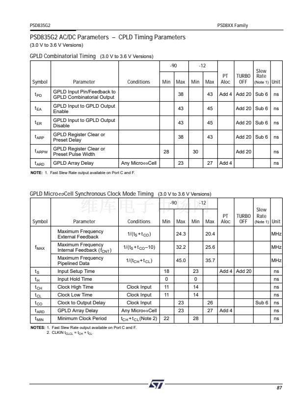
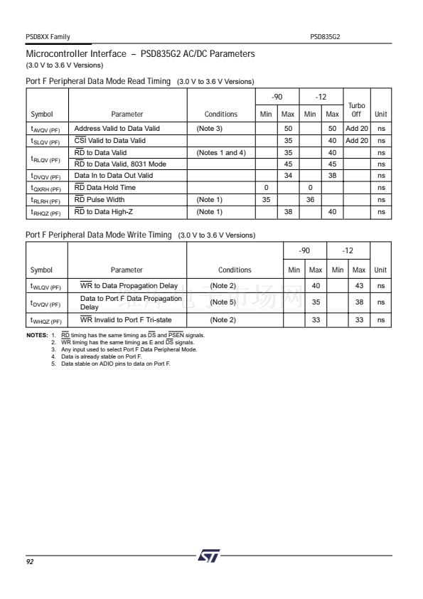
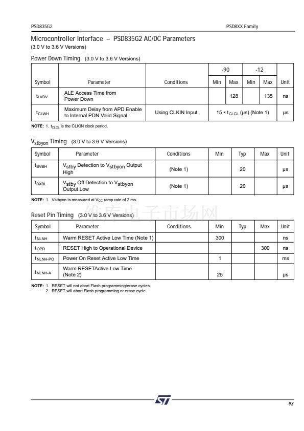
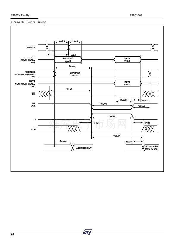
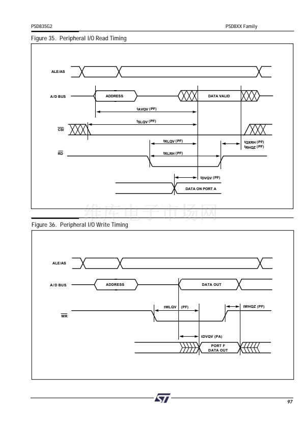
PSD8XX Family
PSD835G2
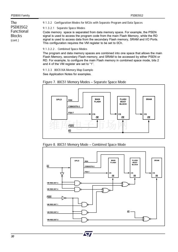
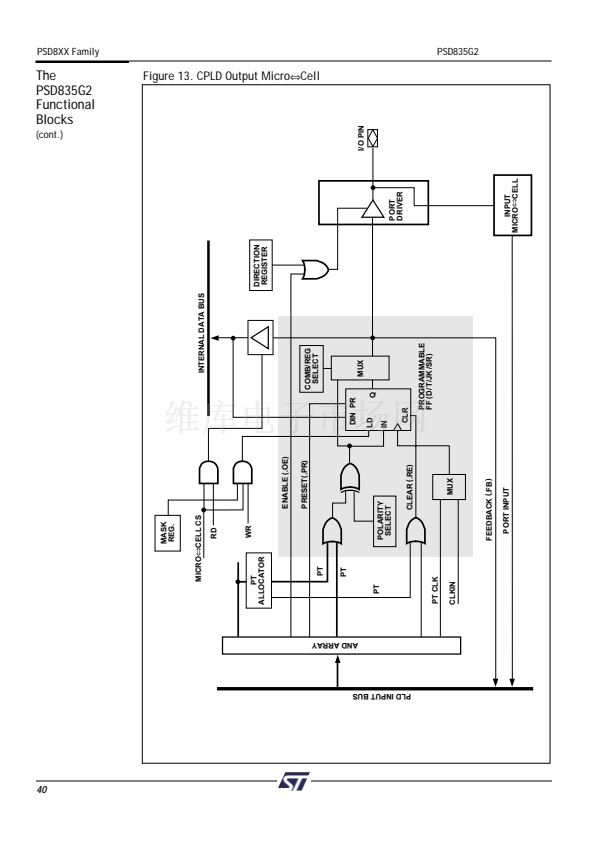
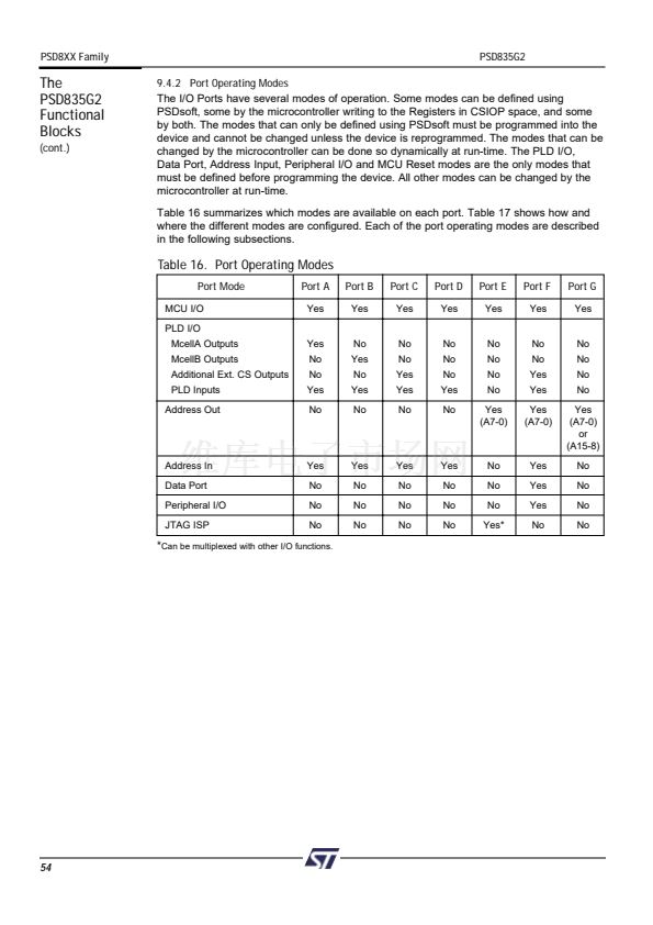
The
PSD835G2
Functional
Blocks
(cont.)
9.1.2 SRAM
The SRAM is enabled when RS0鈥?the SRAM chip select output from the DPLD鈥?is high.
RS0 can contain up to three product terms, allowing flexible memory mapping.
The SRAM can be backed up using an external battery. The external battery should be
connected to the Vstby pin (PE6). If you have an external battery connected to the
PSD835G2, the contents of the SRAM will be retained in the event of a power loss. The
contents of the SRAM will be retained so long as the battery voltage remains at 2V or
greater. If the supply voltage falls below the battery voltage, an internal power switchover
to the battery occurs.
Pin PE7 can be configured as an output that indicates when power is being drawn from the
external battery. This Vbaton signal will be high with the supply voltage falls below the bat-
tery voltage and the battery on PE6 is supplying power to the internal SRAM.
The chip select signal (RS0) for the SRAM, Vstby, and Vbaton are all configured using
PSDsoft.
9.1.3 Memory Select Signals
The main Flash (FSi), secondary Flash (CSBOOTi), and SRAM (RS0) memory select
signals are all outputs of the DPLD. They are defined using PSDsoft. The following rules
apply to the equations for the internal chip select signals:
1. Main Flash memory and secondary Flash memory sector select signals must
not
be
larger than the physical sector size.
2. Any main Flash memory sector must
not
be mapped in the same memory space as
another Main Flash sector.
3. A secondary Flash memory sector must
not
be mapped in the same memory space as
another Flash Boot sector.
4. SRAM and I/O spaces must
not
overlap.
5. A secondary Flash memory sector
may
overlap a main Flash memory sector. In case of
overlap, priority will be given to the Flash Boot sector.
6. SRAM and I/O spaces
may
overlap any other memory sector. Priority will be given to
the SRAM and I/O.
Example
FS0 is valid when the address is in the range of 8000h to BFFFh, CSBOOT0 is valid from
8000h to 9FFFh, and RS0 is valid from 8000h to 87FFh. Any address in the range of RS0
will always access the SRAM. Any address in the range of CSBOOT0 greater than 87FFh
(and less than 9FFFh) will automatically address Boot memory segment 0. Any address
greater than 9FFFh will access the Flash memory segment 0. You can see that half of the
Flash memory segment 0 and one-fourth of Boot segment 0 can not be accessed in this
example. Also note that an equation that defined FS1 to anywhere in the range of 8000h to
BFFFh would
not
be valid.
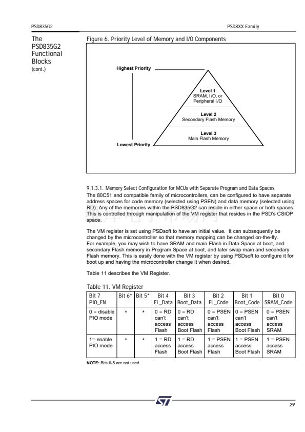
Figure 6 shows the priority levels for all memory components. Any component on a higher
level can overlap and has priority over any component on a lower level. Components on
the same level must
not
overlap. Level one has the highest priority and level 3 has the
lowest.
28


 1
1
 2
2
 3
3
 4
4
 5
5
 6
6
 7
7
 8
8
 9
9
 10
10
 11
11
 12
12
 13
13
 14
14
 15
15
 16
16
 17
17
 18
18
 19
19
 20
20
 21
21
 22
22
 23
23
 24
24
 25
25
 26
26
 27
27
 28
28
 29
29
 30
30
 31
31
 32
32
 33
33
 34
34
 35
35
 36
36
 37
37
 38
38
 39
39
 40
40
 41
41
 42
42
 43
43
 44
44
 45
45
 46
46
 47
47
 48
48
 49
49
 50
50
 51
51
 52
52
 53
53
 54
54
 55
55
 56
56
 57
57
 58
58
 59
59
 60
60
 61
61
 62
62
 63
63
 64
64
 65
65
 66
66
 67
67
 68
68
 69
69
 70
70
 71
71
 72
72
 73
73
 74
74
 75
75
 76
76
 77
77
 78
78
 79
79
 80
80
 81
81
 82
82
 83
83
 84
84
 85
85
 86
86
 87
87
 88
88
 89
89
 90
90
 91
91
 92
92
 93
93
 94
94
 95
95
 96
96
 97
97
 98
98
 99
99
 100
100
 101
101
 102
102
 103
103
 104
104
 105
105
 106
106
 107
107
 108
108
 109
109
 110
110
