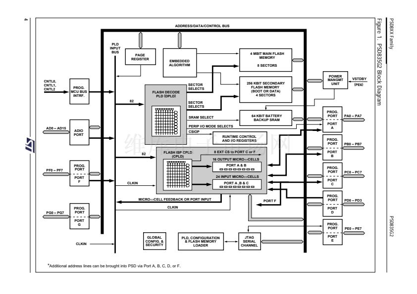
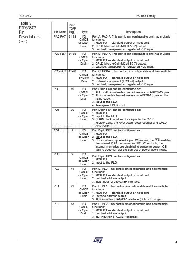
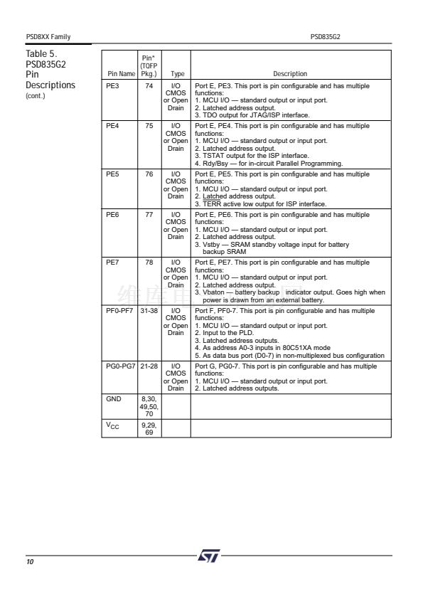
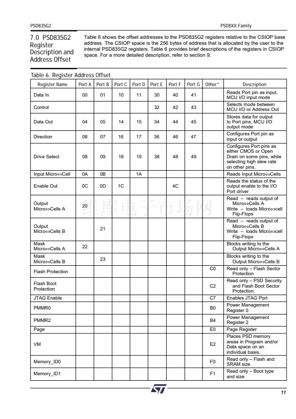
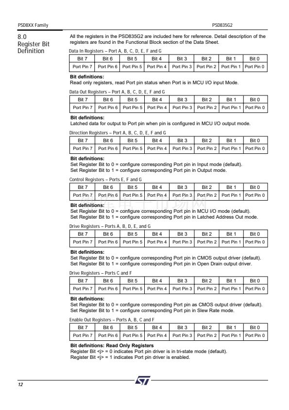
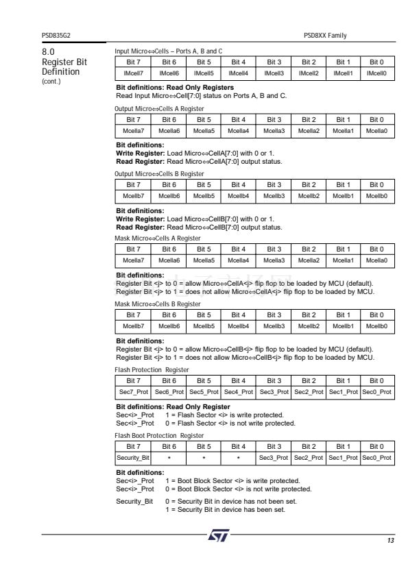
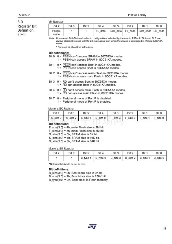
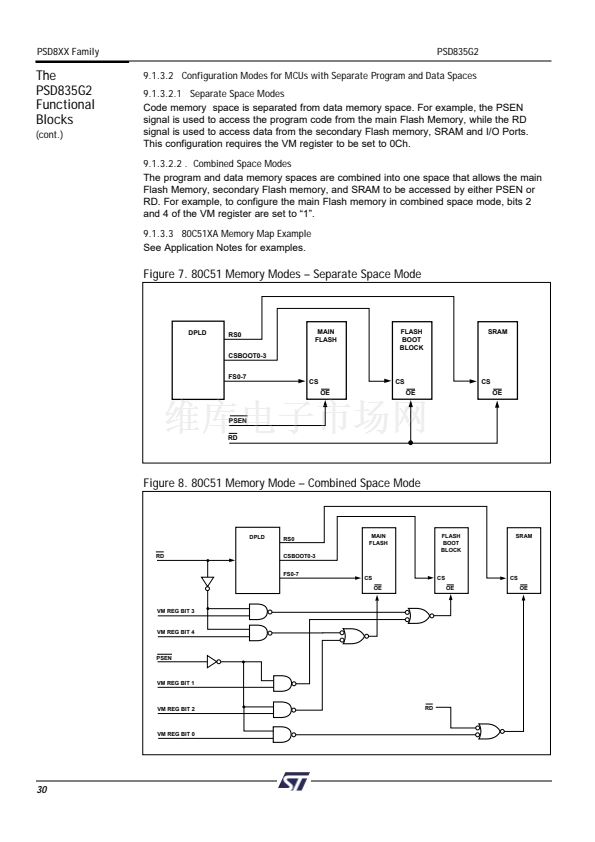
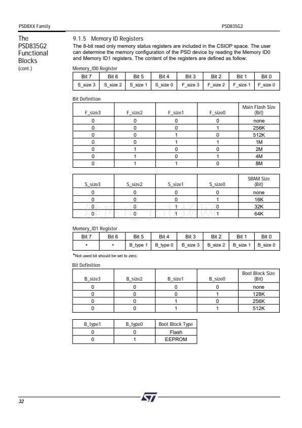
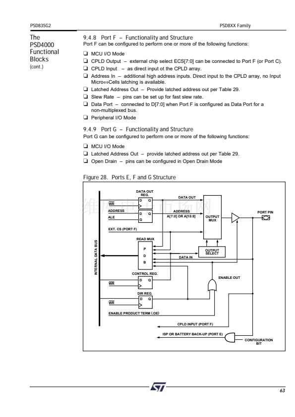
鈥?/div>
SRAM.
The memory select signals for these blocks originate from the Decode PLD (DPLD) and
are user-defined in PSDsoft.
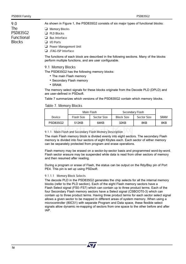
Table 7 summarizes which versions of the PSD835G2 contain which memory blocks.
Table 7. Memory Blocks
Main Flash
Device
PSD835G2
Secondary Flash
Block Size
32KB
Flash Size
512KB
Sector Size
64KB
Sector Size
8KB
SRAM
8KB
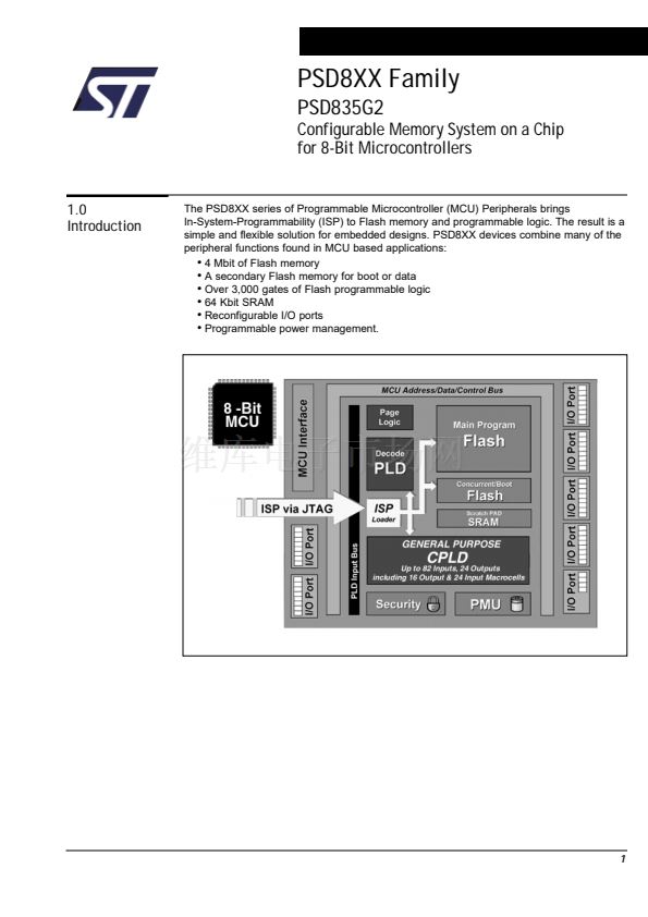
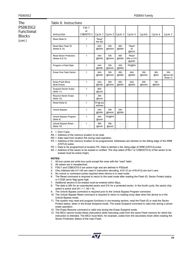
9.1.1 Main Flash and Secondary Flash Memory Description
The main Flash memory block is divided evenly into eight sectors. The secondary Flash
memory is divided into four sectors of eight Kbytes each. Each sector of either memory
can be separately protected from program and erase operations.
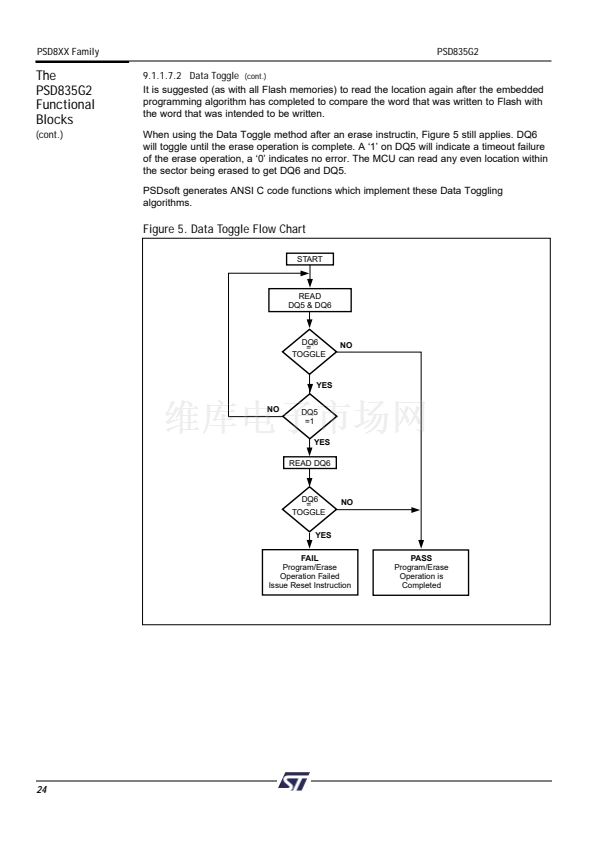
Flash memory may be erased on a sector-by-sector basis and programmed word-by-word.
Flash sector erasure may be suspended while data is read from other sectors of memory
and then resumed after reading.
During a program or erase of Flash, the status can be output on the Rdy/Bsy pin of Port
PE4. This pin is set up using PSDsoft.
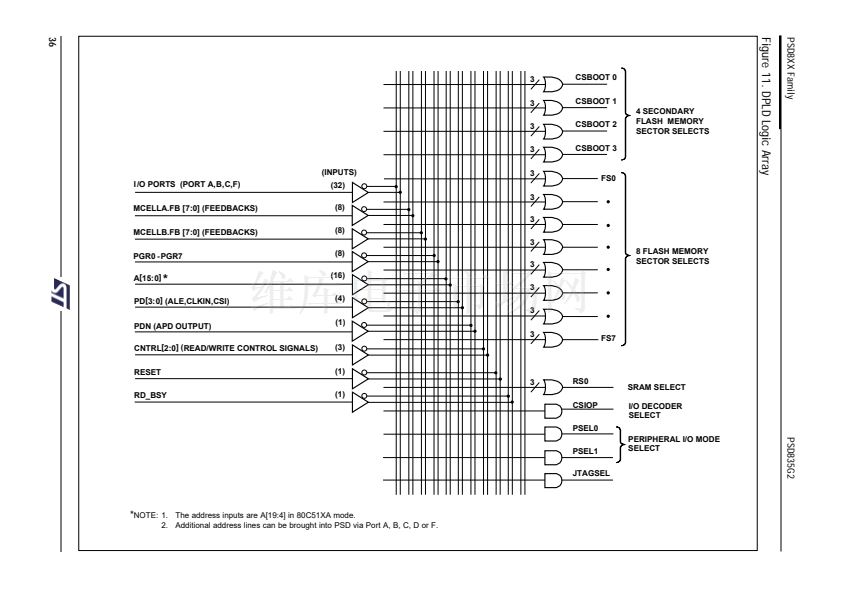
9.1.1.1 Memory Block Selects
The decode PLD in the PSD835G2 generates the chip selects for all the internal memory
blocks (refer to the PLD section). Each of the eight Flash memory sectors have a
Flash Select signal (FS0-FS7) which can contain up to three product terms. Each of the
four Secondary Flash memory sectors have a Select signal (CSBOOT0-3) which can
contain up to three product terms. Having three product terms for each sector select signal
allows a given sector to be mapped in different areas of system memory. When using a
microcontroller (80C51) with separate Program and Data space, these flexible select
signals allow dynamic re-mapping of sectors from one space to the other before and after
IAP.
16


 1
1
 2
2
 3
3
 4
4
 5
5
 6
6
 7
7
 8
8
 9
9
 10
10
 11
11
 12
12
 13
13
 14
14
 15
15
 16
16
 17
17
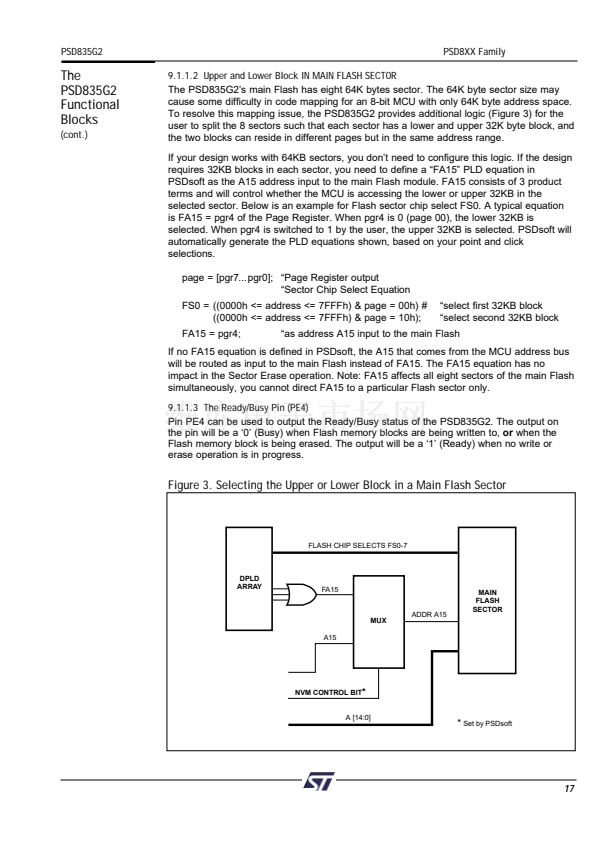 18
18
 19
19
 20
20
 21
21
 22
22
 23
23
 24
24
 25
25
 26
26
 27
27
 28
28
 29
29
 30
30
 31
31
 32
32
 33
33
 34
34
 35
35
 36
36
 37
37
 38
38
 39
39
 40
40
 41
41
 42
42
 43
43
 44
44
 45
45
 46
46
 47
47
 48
48
 49
49
 50
50
 51
51
 52
52
 53
53
 54
54
 55
55
 56
56
 57
57
 58
58
 59
59
 60
60
 61
61
 62
62
 63
63
 64
64
 65
65
 66
66
 67
67
 68
68
 69
69
 70
70
 71
71
 72
72
 73
73
 74
74
 75
75
 76
76
 77
77
 78
78
 79
79
 80
80
 81
81
 82
82
 83
83
 84
84
 85
85
 86
86
 87
87
 88
88
 89
89
 90
90
 91
91
 92
92
 93
93
 94
94
 95
95
 96
96
 97
97
 98
98
 99
99
 100
100
 101
101
 102
102
 103
103
 104
104
 105
105
 106
106
 107
107
 108
108
 109
109
 110
110
