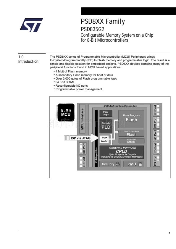
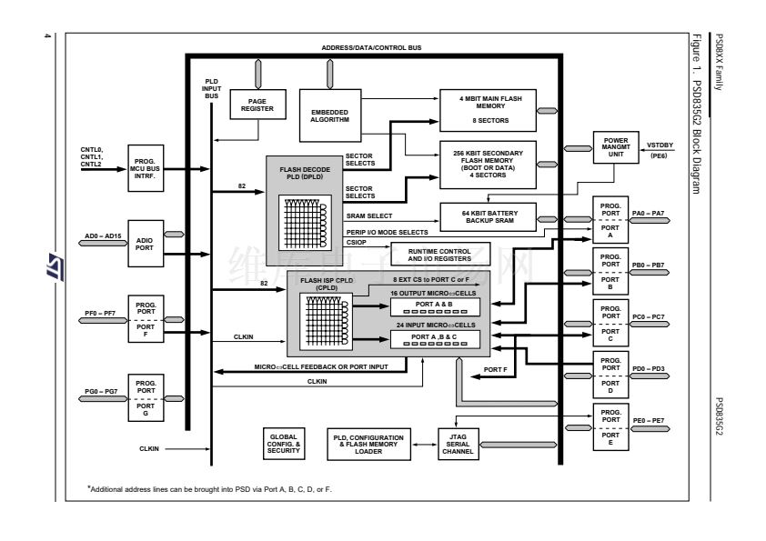
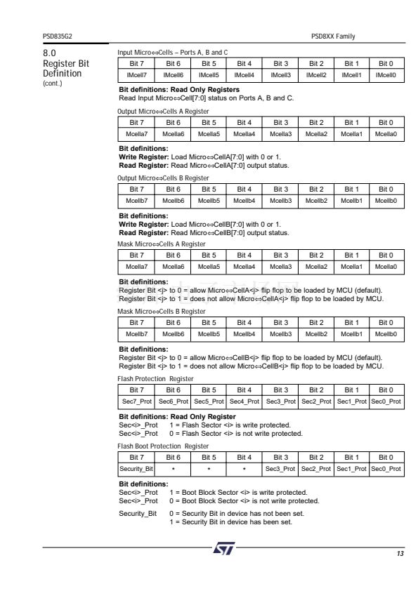
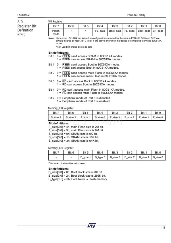
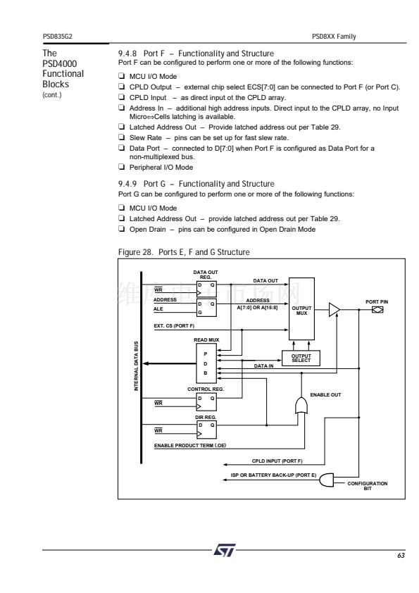
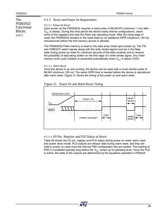
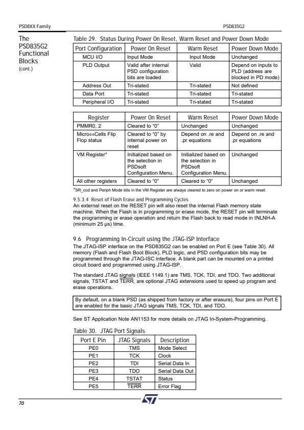
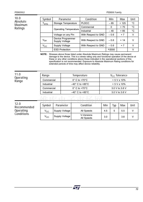
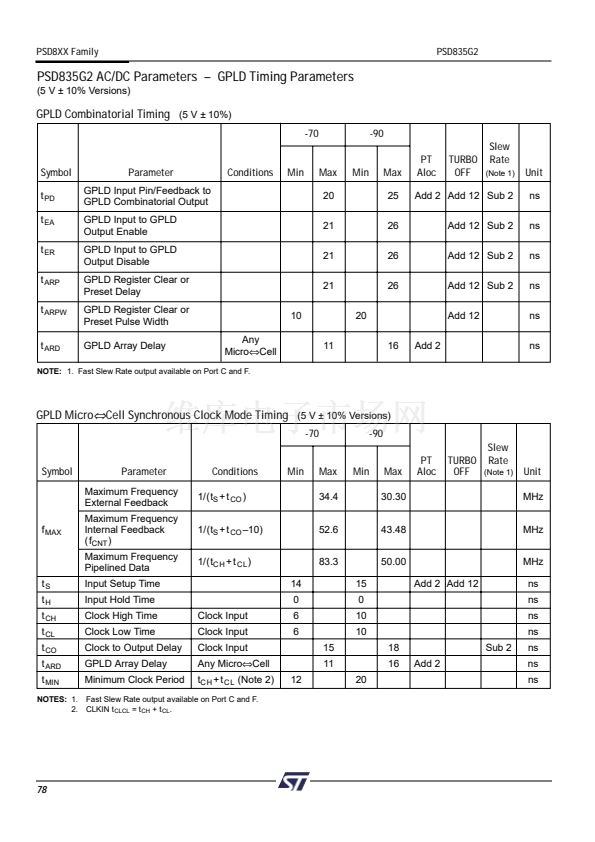
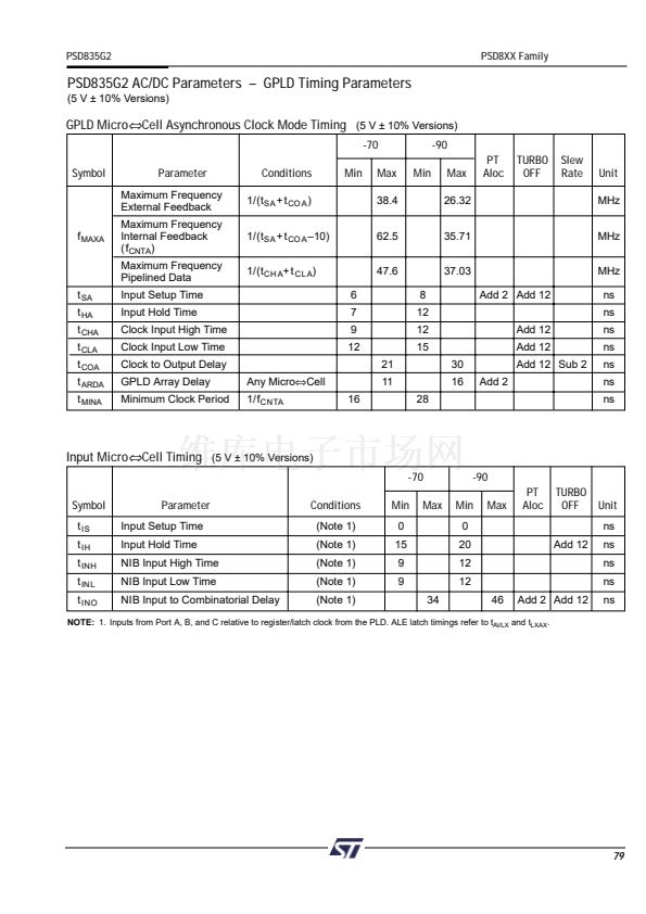
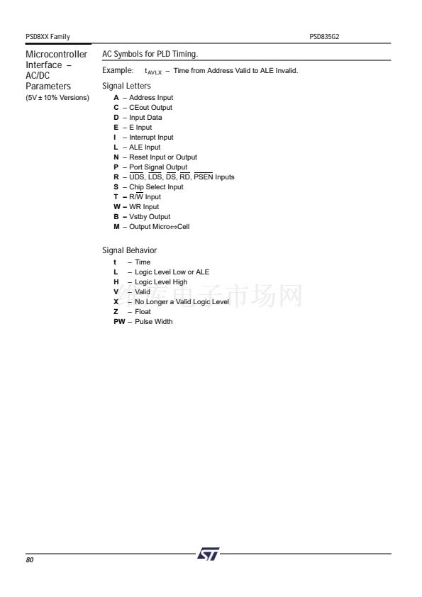
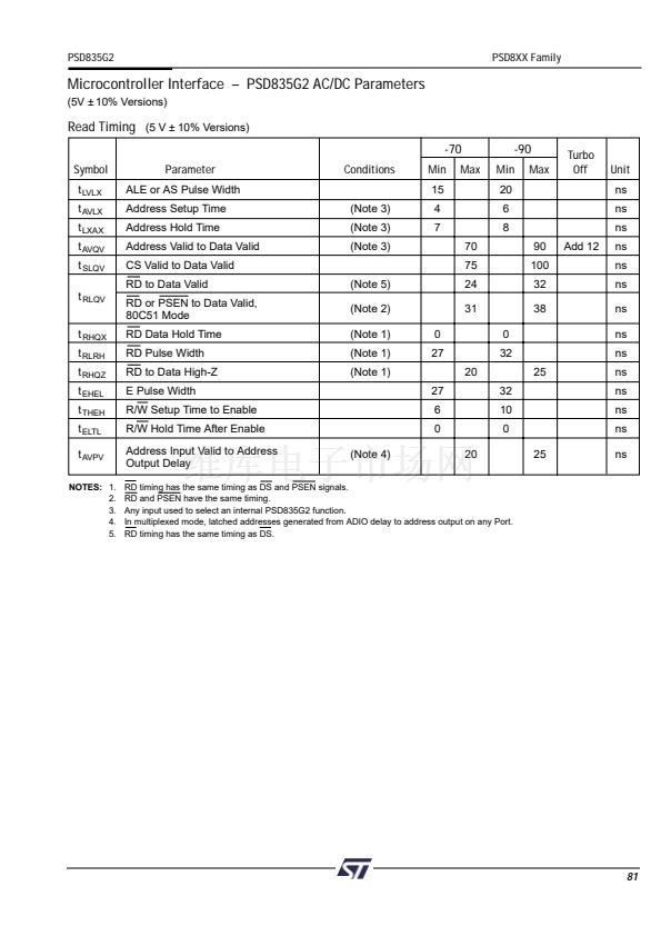
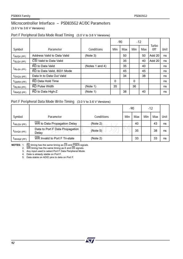
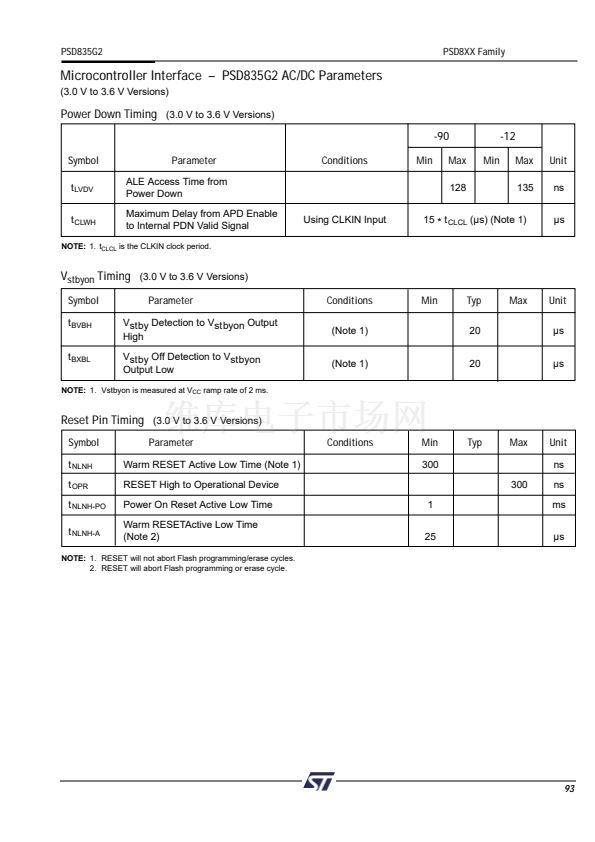
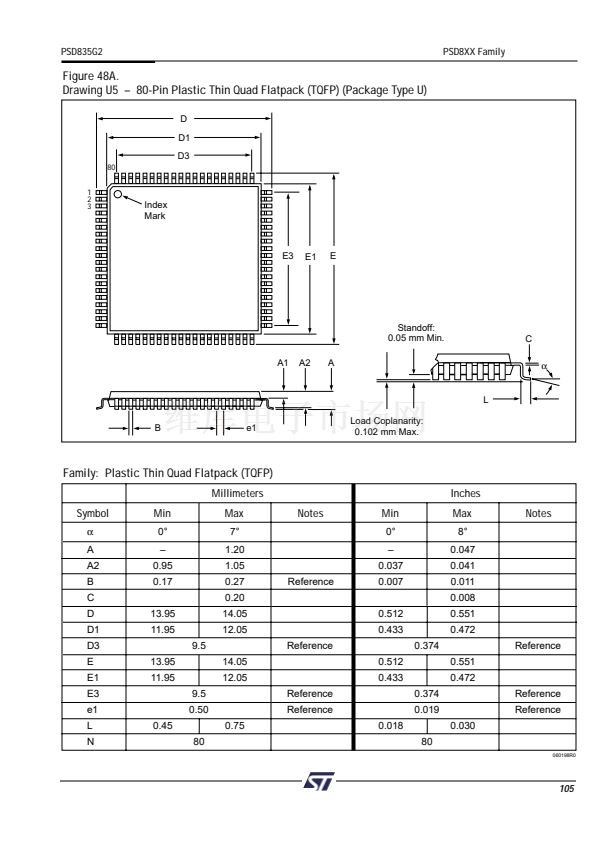
PSD835G2
PSD8XX Family
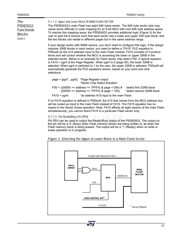
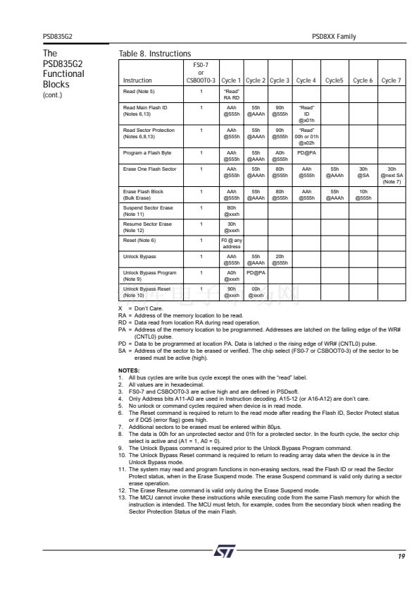
9.1.1.2 Upper and Lower Block IN MAIN FLASH SECTOR
The PSD835G2鈥檚 main Flash has eight 64K bytes sector. The 64K byte sector size may
cause some difficulty in code mapping for an 8-bit MCU with only 64K byte address space.
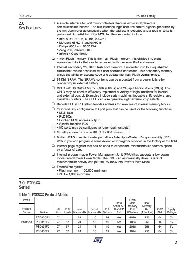
To resolve this mapping issue, the PSD835G2 provides additional logic (Figure 3) for the
user to split the 8 sectors such that each sector has a lower and upper 32K byte block, and
the two blocks can reside in different pages but in the same address range.
If your design works with 64KB sectors, you don鈥檛 need to configure this logic. If the design
requires 32KB blocks in each sector, you need to define a 鈥淔A15鈥?PLD equation in
PSDsoft as the A15 address input to the main Flash module. FA15 consists of 3 product
terms and will control whether the MCU is accessing the lower or upper 32KB in the
selected sector. Below is an example for Flash sector chip select FS0. A typical equation
is FA15 = pgr4 of the Page Register. When pgr4 is 0 (page 00), the lower 32KB is
selected. When pgr4 is switched to 1 by the user, the upper 32KB is selected. PSDsoft will
automatically generate the PLD equations shown, based on your point and click
selections.
page = [pgr7...pgr0]; 鈥淧age Register output
鈥淪ector Chip Select Equation
FS0 = ((0000h <= address <= 7FFFh) & page = 00h) #
((0000h <= address <= 7FFFh) & page = 10h);
FA15 = pgr4;
鈥渟elect first 32KB block
鈥渟elect second 32KB block
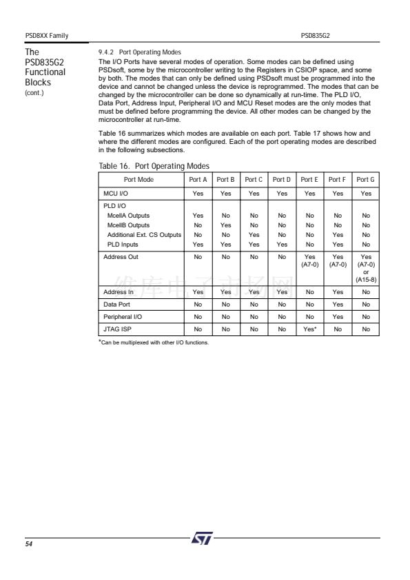
The
PSD835G2
Functional
Blocks
(cont.)
鈥渁s address A15 input to the main Flash
If no FA15 equation is defined in PSDsoft, the A15 that comes from the MCU address bus
will be routed as input to the main Flash instead of FA15. The FA15 equation has no
impact in the Sector Erase operation. Note: FA15 affects all eight sectors of the main Flash
simultaneously, you cannot direct FA15 to a particular Flash sector only.
9.1.1.3 The Ready/Busy Pin (PE4)
Pin PE4 can be used to output the Ready/Busy status of the PSD835G2. The output on
the pin will be a 鈥?鈥?(Busy) when Flash memory blocks are being written to,
or
when the
Flash memory block is being erased. The output will be a 鈥?鈥?(Ready) when no write or
erase operation is in progress.
Figure 3. Selecting the Upper or Lower Block in a Main Flash Sector
FLASH CHIP SELECTS FS0-7
DPLD
ARRAY
FA15
MUX
A15
ADDR A15
MAIN
FLASH
SECTOR
NVM CONTROL BIT
*
A [14:0]
*
Set by PSDsoft
17


 1
1
 2
2
 3
3
 4
4
 5
5
 6
6
 7
7
 8
8
 9
9
 10
10
 11
11
 12
12
 13
13
 14
14
 15
15
 16
16
 17
17
 18
18
 19
19
 20
20
 21
21
 22
22
 23
23
 24
24
 25
25
 26
26
 27
27
 28
28
 29
29
 30
30
 31
31
 32
32
 33
33
 34
34
 35
35
 36
36
 37
37
 38
38
 39
39
 40
40
 41
41
 42
42
 43
43
 44
44
 45
45
 46
46
 47
47
 48
48
 49
49
 50
50
 51
51
 52
52
 53
53
 54
54
 55
55
 56
56
 57
57
 58
58
 59
59
 60
60
 61
61
 62
62
 63
63
 64
64
 65
65
 66
66
 67
67
 68
68
 69
69
 70
70
 71
71
 72
72
 73
73
 74
74
 75
75
 76
76
 77
77
 78
78
 79
79
 80
80
 81
81
 82
82
 83
83
 84
84
 85
85
 86
86
 87
87
 88
88
 89
89
 90
90
 91
91
 92
92
 93
93
 94
94
 95
95
 96
96
 97
97
 98
98
 99
99
 100
100
 101
101
 102
102
 103
103
 104
104
 105
105
 106
106
 107
107
 108
108
 109
109
 110
110
