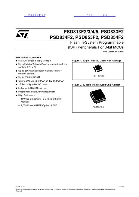
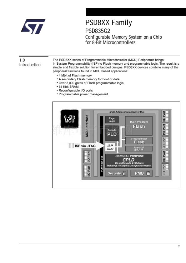
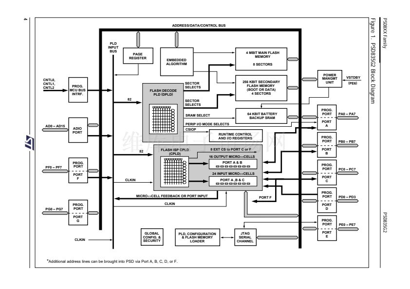
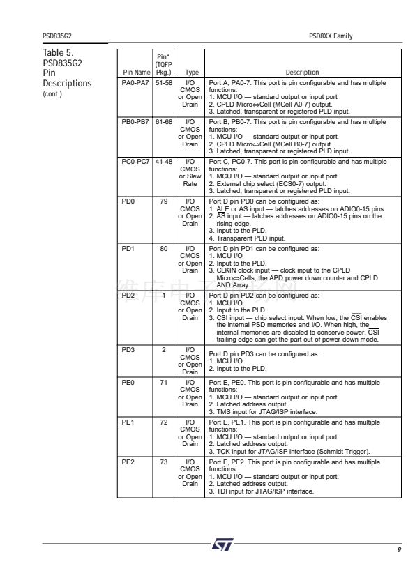
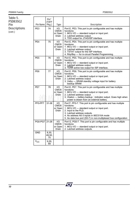
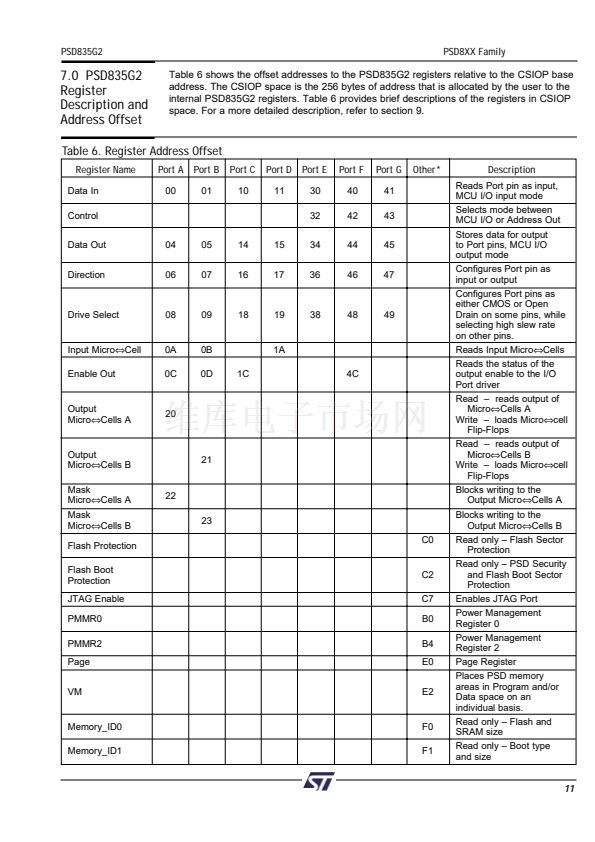
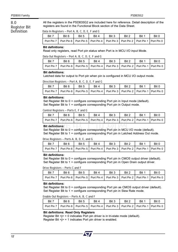
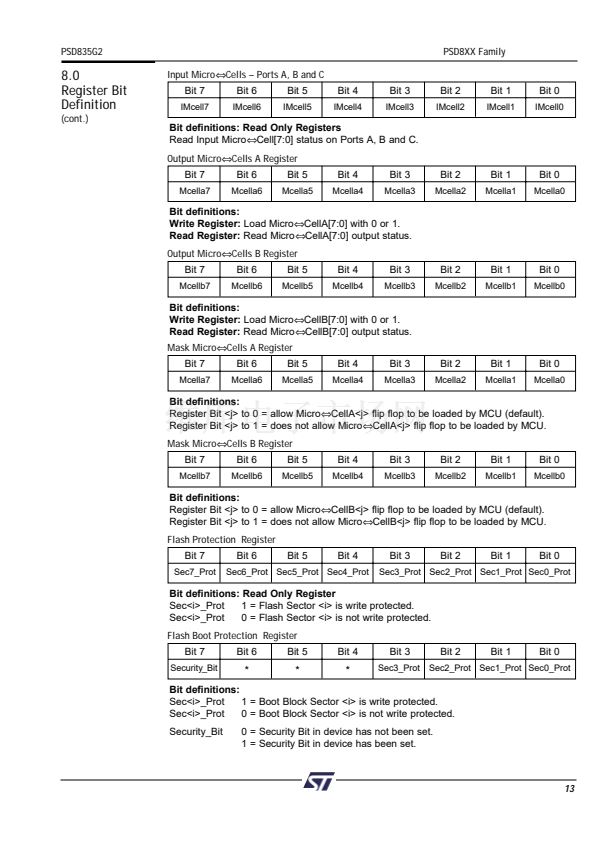
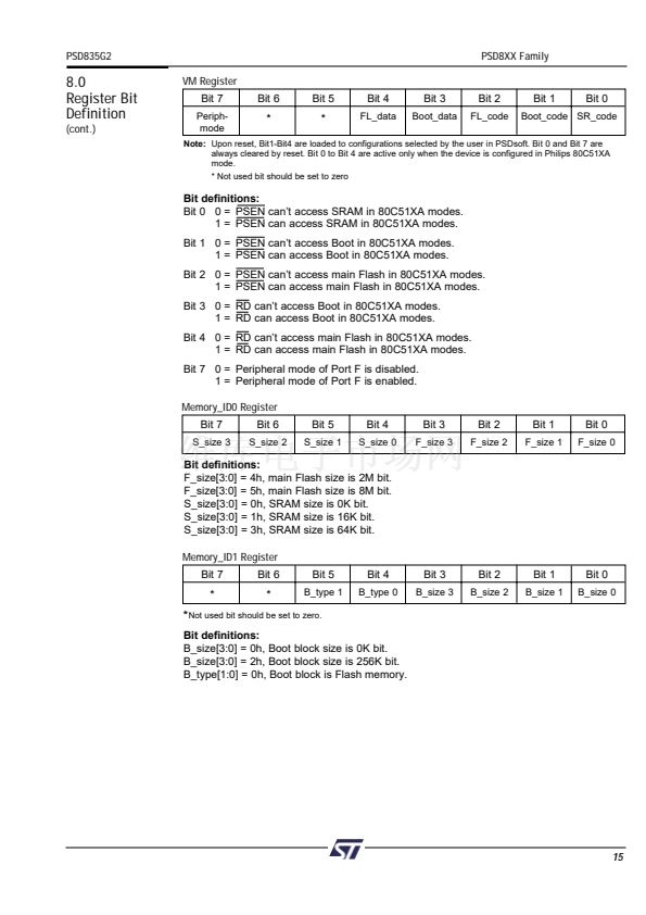
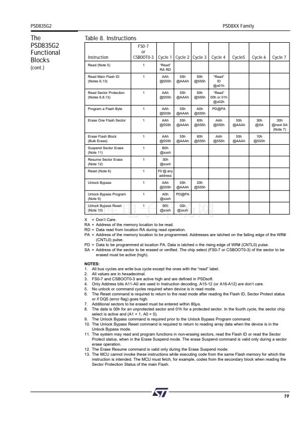
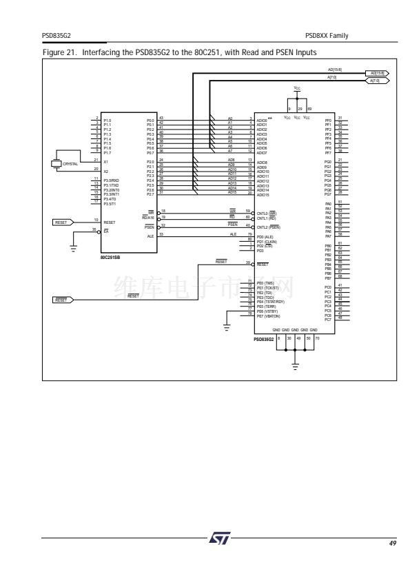
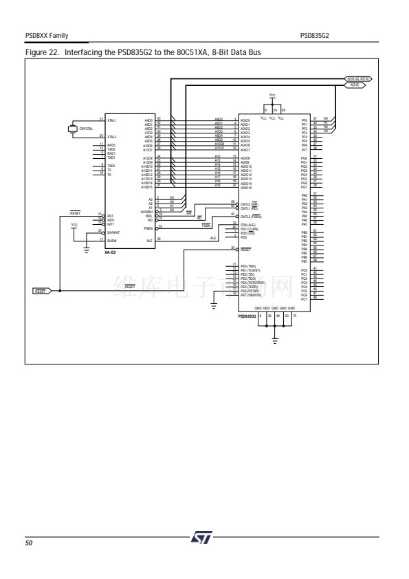
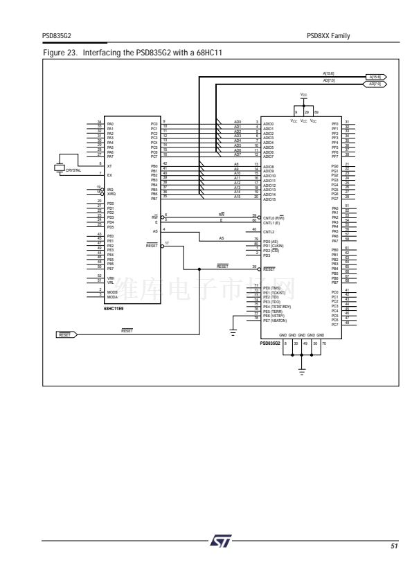
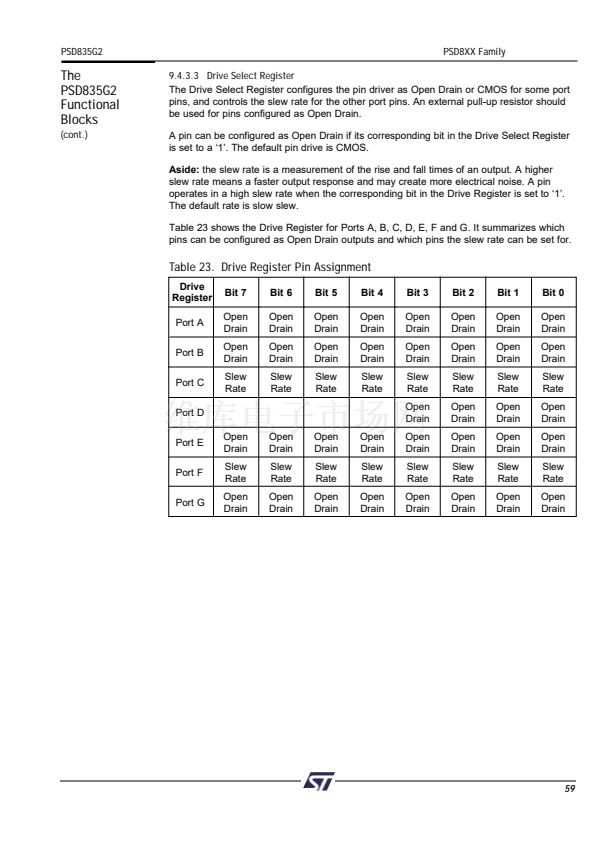
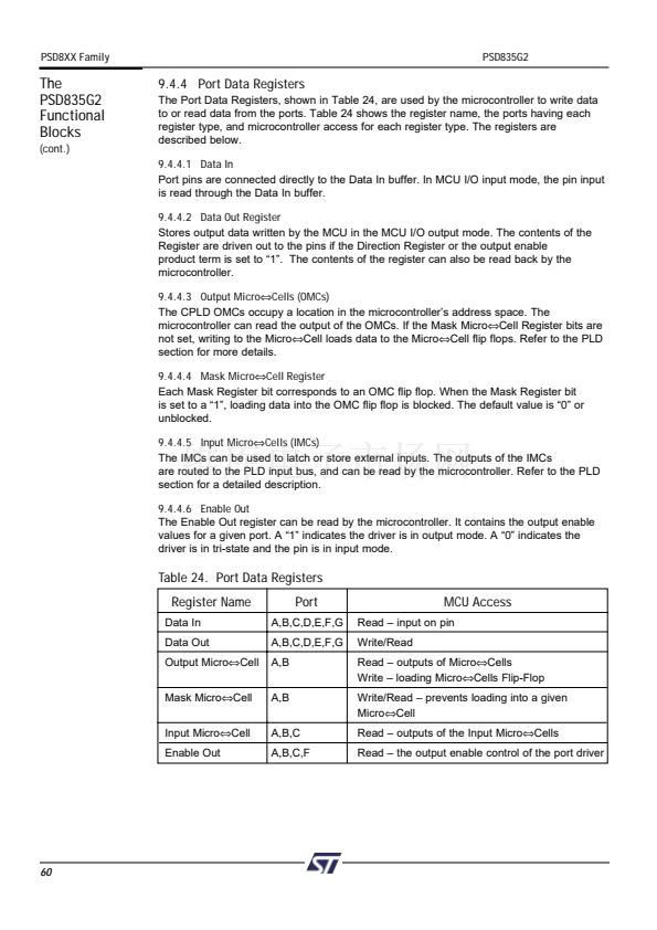
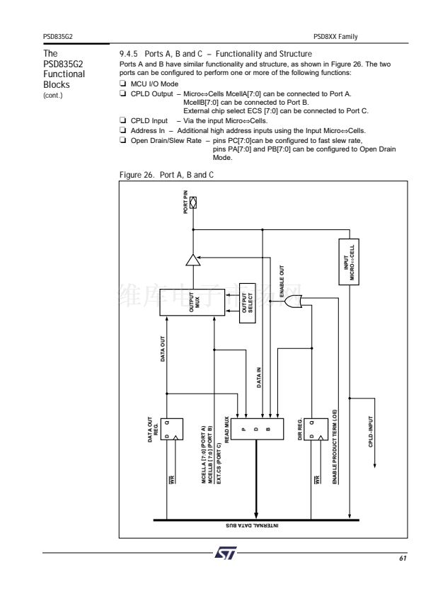
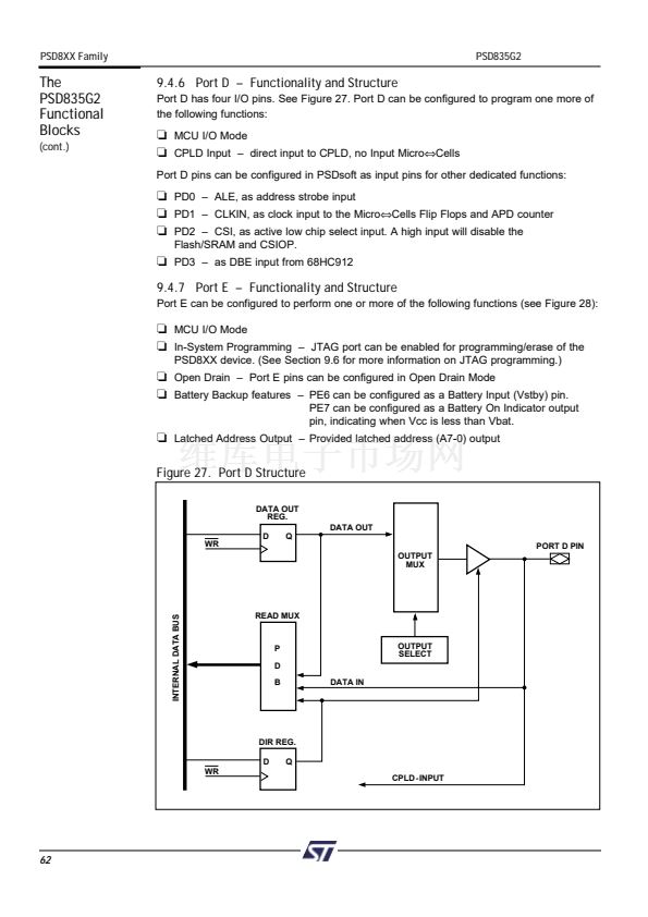
PSD8XX Family
PSD835G2
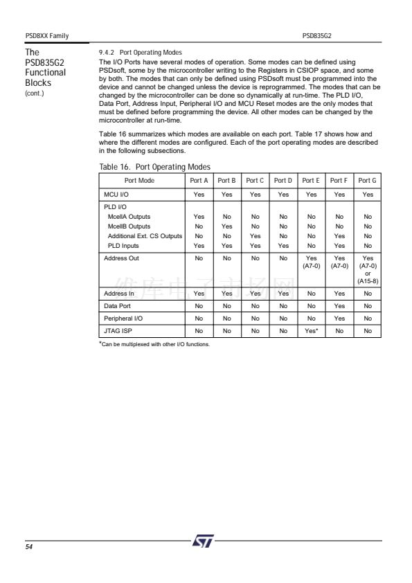
The
PSD835G2
Functional
Blocks
(cont.)
9.1.1.7 Programming Flash Memory
Flash memory must be erased prior to being programmed. The MCU may erase Flash
memory all at once or by-sector. Flash memory sector erases to all logic ones (FF hex),
and its bits are programmed to logic zeros. Although erasing Flash memory occurs on a
sector basis, programming Flash memory occurs on a word basis.
The PSD835G2 main Flash and secondary Flash memories require the MCU to send an
instruction to program a word or perform an erase function (see Table 8).
Once the MCU issues a Flash memory program or erase instruction, it must check for the
status of completion. The embedded algorithms that are invoked inside the PSD835G2
support several means to provide status to the MCU. Status may be checked using any of
three methods: Data Polling, Data Toggle, or the Ready/Busy output pin.
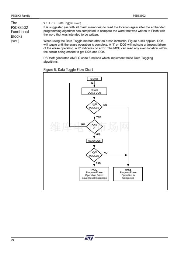
9.1.1.7.1 Data Polling
Polling on DQ7 is a method of checking whether a Program or Erase instruction is in
progress or has completed. Figure 4 shows the Data Polling algorithm.
When the MCU issues a programming instruction, the embedded algorithm within the
PSD835G2 begins. The MCU then reads the location of the word to be programmed in
Flash to check status. Data bit DQ7 of this location becomes the compliment of data
bit 7of the original data word to be programmed. The MCU continues to poll this location,
comparing DQ7 and monitoring the Error bit on DQ5. When the DQ7 matches data bit 7 of
the original data, and the Error bit at DQ5 remains 鈥?鈥? then the embedded algorithm is
complete. If the Error bit at DQ5 is 鈥?鈥? the MCU should test DQ7 again since DQ7 may
have changed simultaneously with DQ5 (see Figure 4).
The Error bit at DQ5 will be set if either an internal timeout occurred while the embedded
algorithm attempted to program the location or if the MCU attempted to program a 鈥?鈥?to a
bit that was not erased (not erased is logic 鈥?鈥?.
It is suggested (as with all Flash memories) to read the location again after the embedded
programming algorithm has completed to compare the word that was written to Flash with
the word that was intended to be written.
When using the Data Polling method after an erase instruction, Figure 4 still applies.
However, DQ7 will be 鈥?鈥?until the erase operation is complete. A 鈥?鈥?on DQ5 will indicate
a timeout failure of the erase operation, a 鈥?鈥?indicates no error. The MCU can read any
location within the sector being erased to get DQ7 and DQ5.
PSDsoft generates ANSI C code functions which implement these Data Polling
algorithms.
22


 1
1
 2
2
 3
3
 4
4
 5
5
 6
6
 7
7
 8
8
 9
9
 10
10
 11
11
 12
12
 13
13
 14
14
 15
15
 16
16
 17
17
 18
18
 19
19
 20
20
 21
21
 22
22
 23
23
 24
24
 25
25
 26
26
 27
27
 28
28
 29
29
 30
30
 31
31
 32
32
 33
33
 34
34
 35
35
 36
36
 37
37
 38
38
 39
39
 40
40
 41
41
 42
42
 43
43
 44
44
 45
45
 46
46
 47
47
 48
48
 49
49
 50
50
 51
51
 52
52
 53
53
 54
54
 55
55
 56
56
 57
57
 58
58
 59
59
 60
60
 61
61
 62
62
 63
63
 64
64
 65
65
 66
66
 67
67
 68
68
 69
69
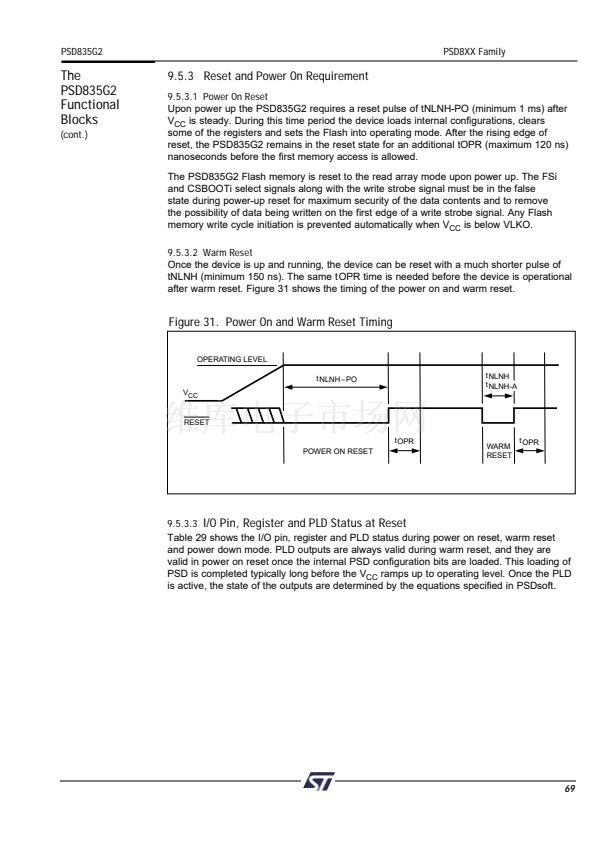 70
70
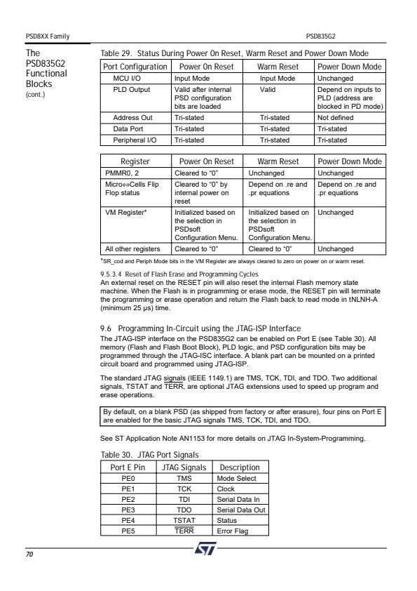 71
71
 72
72
 73
73
 74
74
 75
75
 76
76
 77
77
 78
78
 79
79
 80
80
 81
81
 82
82
 83
83
 84
84
 85
85
 86
86
 87
87
 88
88
 89
89
 90
90
 91
91
 92
92
 93
93
 94
94
 95
95
 96
96
 97
97
 98
98
 99
99
 100
100
 101
101
 102
102
 103
103
 104
104
 105
105
 106
106
 107
107
 108
108
 109
109
 110
110
