PSD835G2
PSD8XX Family
The
PSD835G2
Functional
Blocks
(cont.)
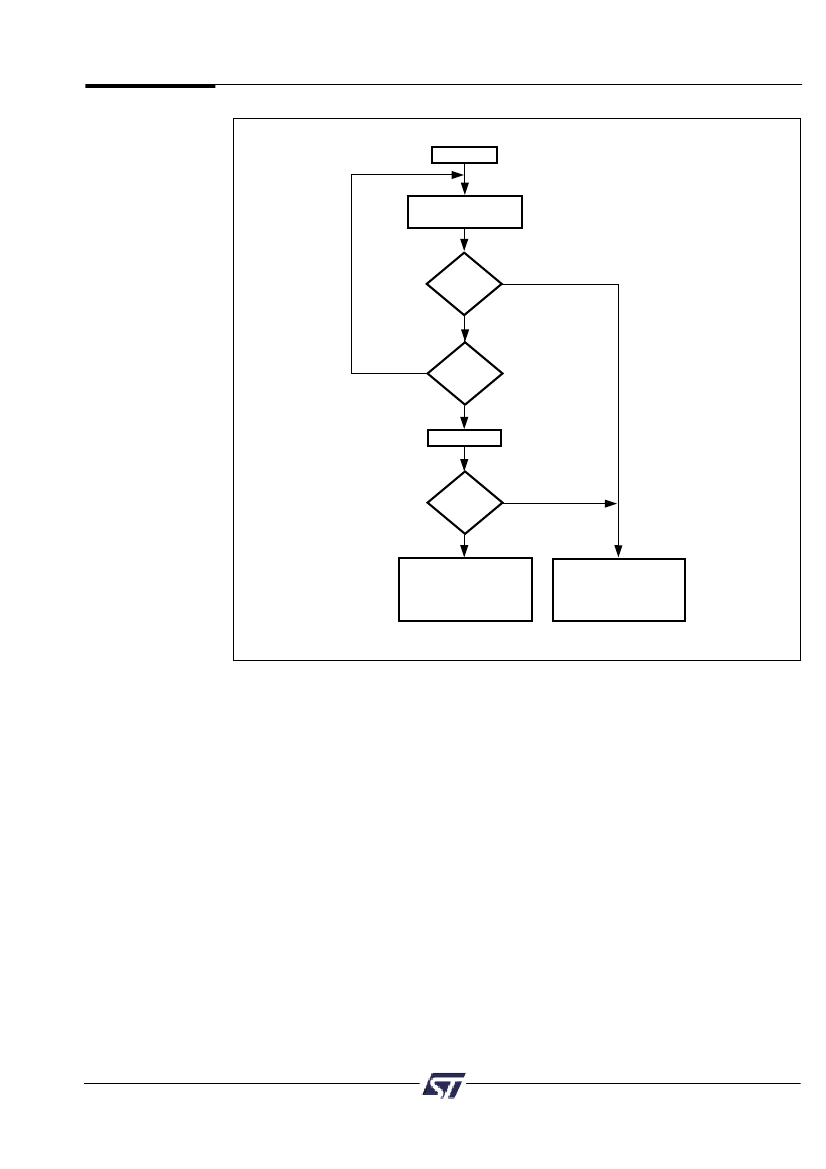
Figure 4. Data Polling Flow Chart
START
READ DQ5 & DQ7
at VALID ADDRESS
DQ7
=
DATA7
NO
NO
YES
DQ5
=1
YES
READ DQ7
DQ7
=
DATA
NO
YES
FAIL
Program/Erase
Operation Failed
Issue Reset Instruction
PASS
Program/Erase
Operation is
Completed
9.1.1.7.2 Data Toggle
Checking the Data Toggle bit on DQ6 is a method of determining whether a Program or
Erase instruction is in progress or has completed. Figure 5 shows the Data Toggle
algorithm.
When the MCU issues a programming instruction, the embedded algorithm within the
PSD835G2 begins. The MCU then reads the location to be programmed in Flash to check
status. Data bit DQ6 of this location will toggle each time the MCU reads this location until
the embedded algorithm is complete. The MCU continues to read this location, checking
DQ6 and monitoring the Error bit on DQ5. When DQ6 stops toggling (two consecutive
reads yield the same value), and the Error bit on DQ5 remains 鈥?鈥? then the embedded
algorithm is complete. If the Error bit on DQ5 is 鈥?鈥? the MCU should test DQ6 again, since
DQ6 may have changed simultaneously with DQ5 (see Figure 5).
The Error bit at DQ5 will be set if either an internal timeout occurred while the embedded
algorithm attempted to program, or if the MCU attempted to program a 鈥?鈥?to a bit that was
not erased (not erased is logic 鈥?鈥?.
23
