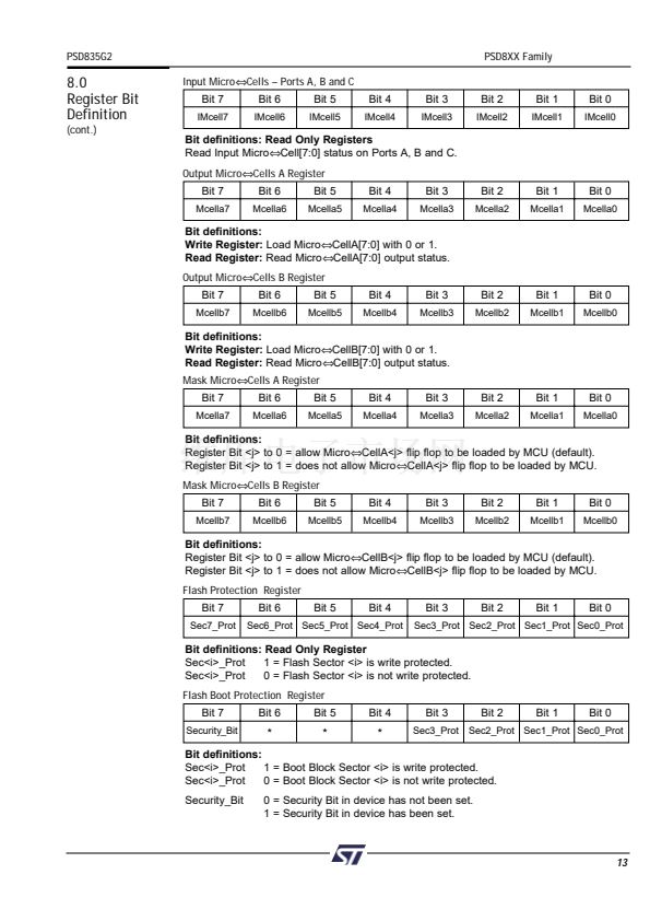
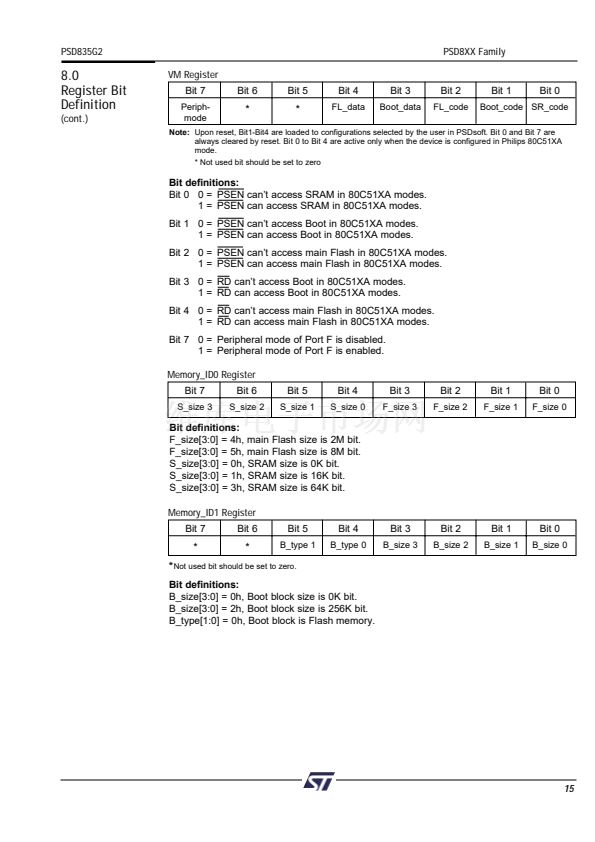
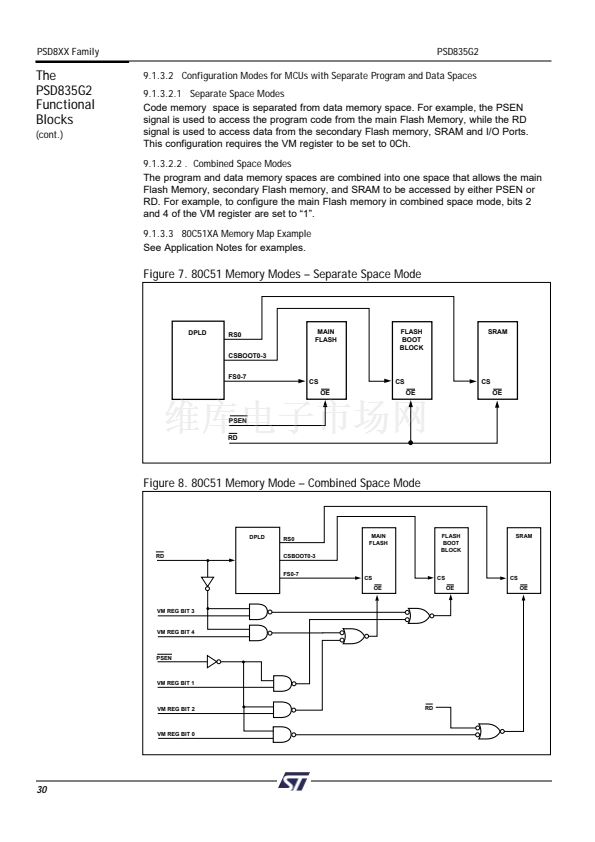
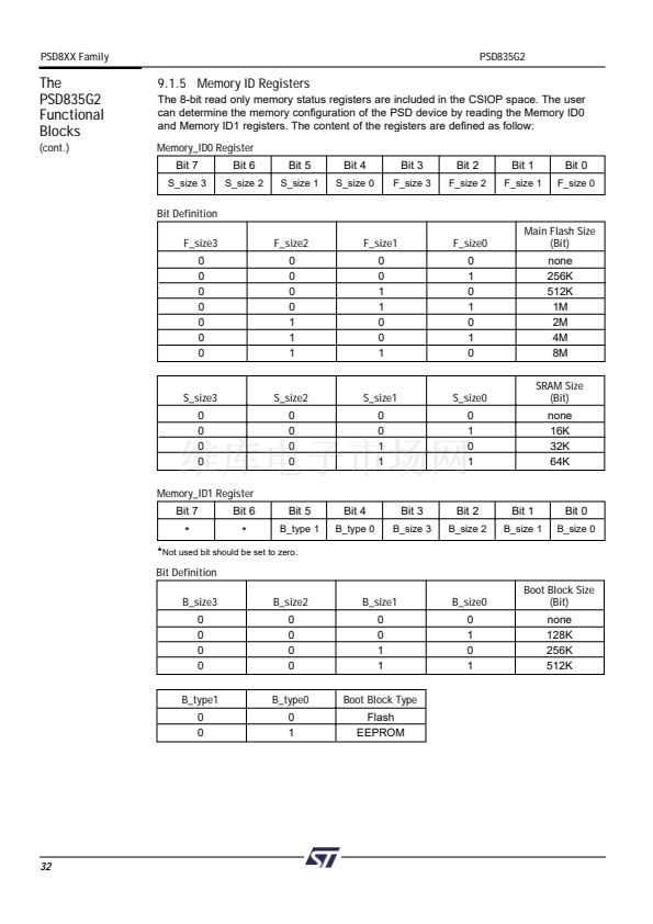
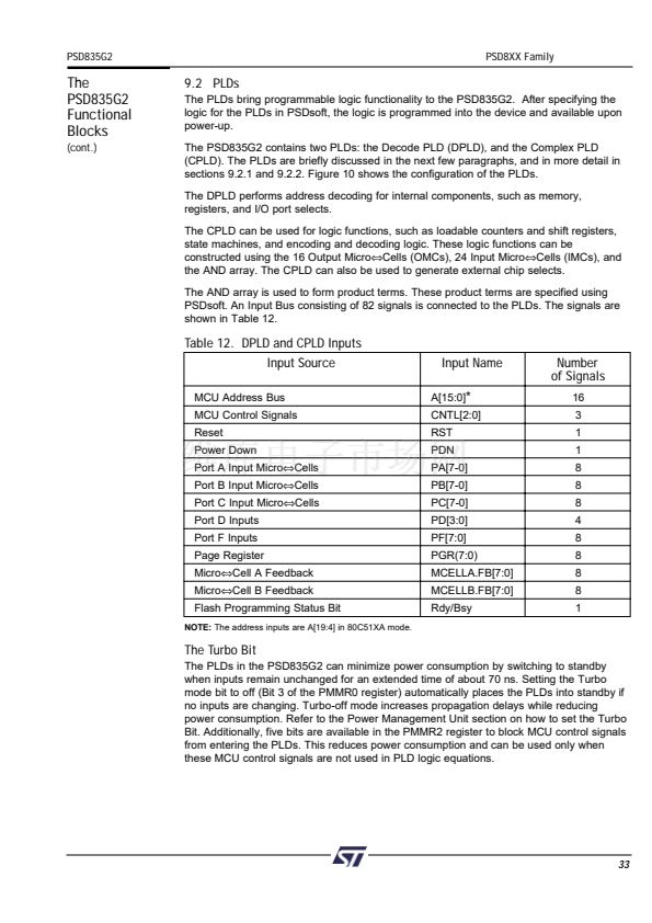
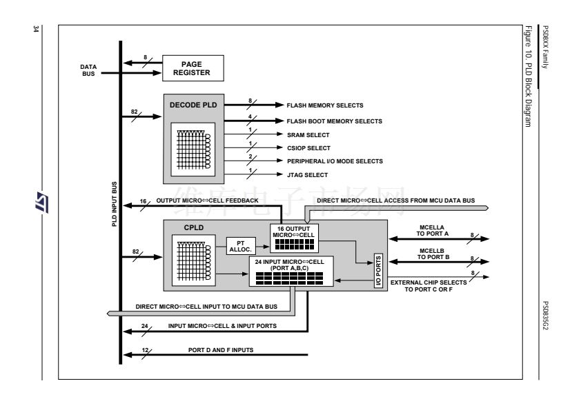
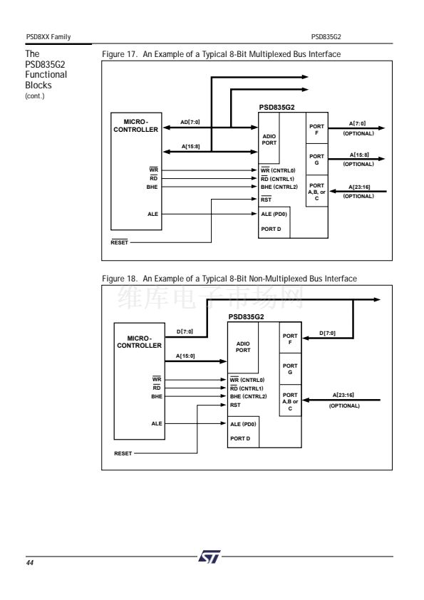
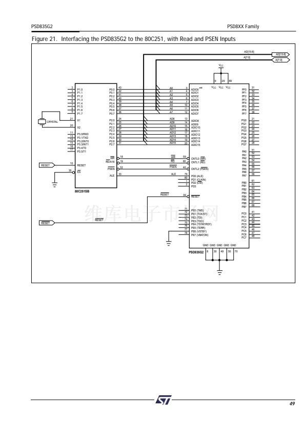
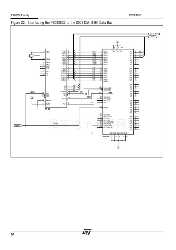
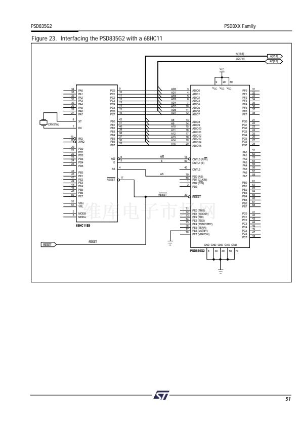
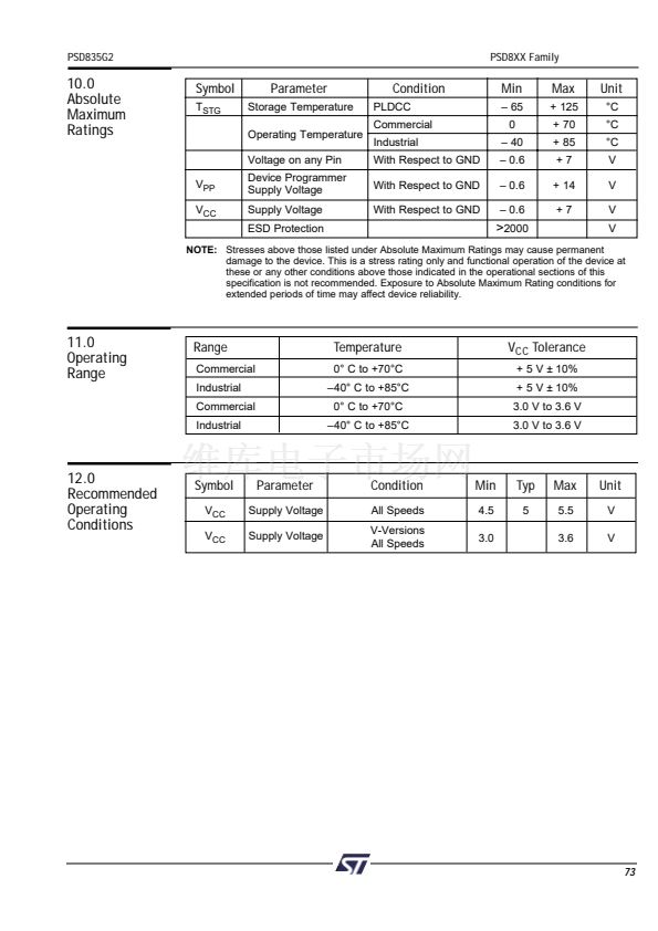
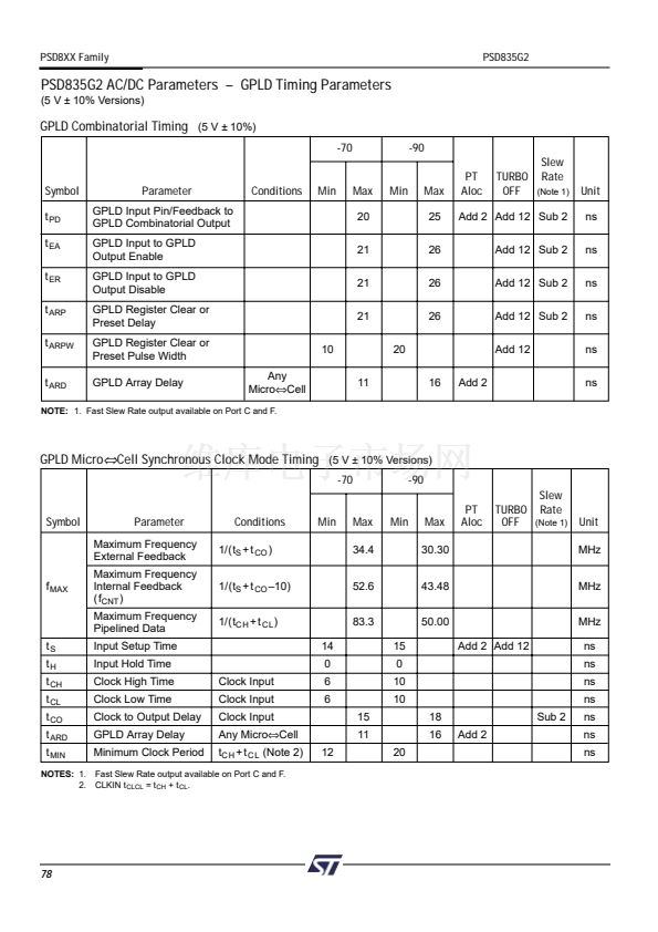
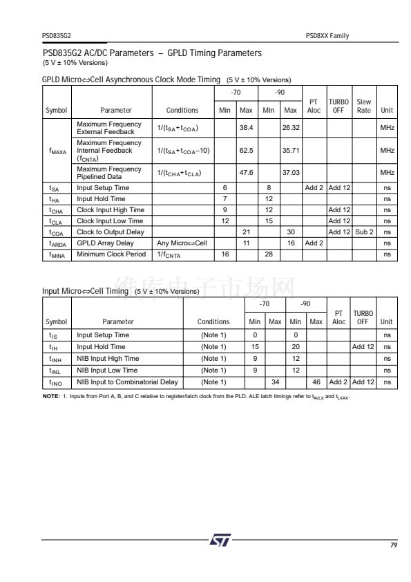
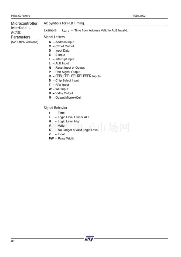
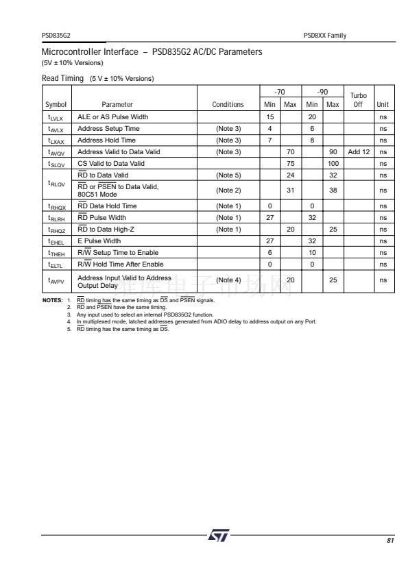
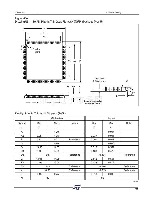
PSD835G2
PSD8XX Family
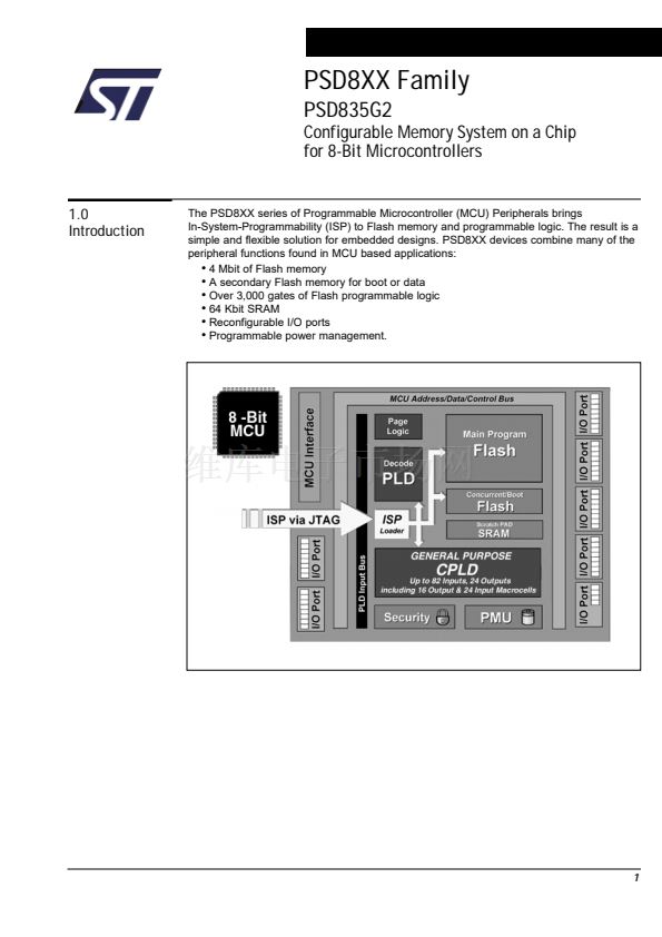
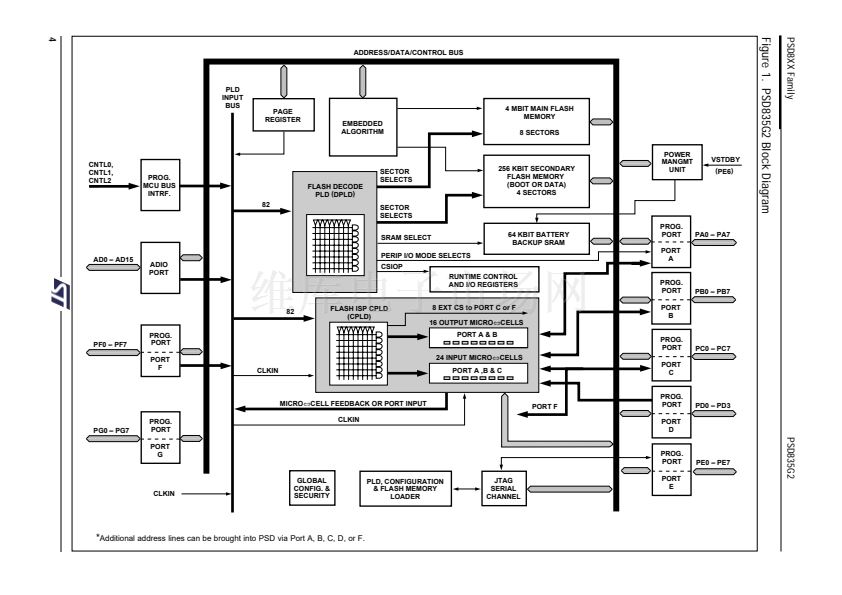
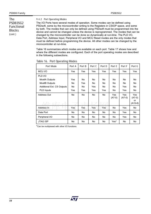
The
PSD835G2
Functional
Blocks
(cont.)
9.1.1.8 Unlock Bypass Instruction
The unlock bypass feature allows the system to program words to the flash memories
faster than using the standard program instruction. The unlock bypass instruction is
initiated by first writing two unlock cycles. This is followed by a third write cycle containing
the unlock bypass command, 20h (see Table 8). The flash memory then enters the unlock
bypass mode. A two-cycle Unlock Bypass Program instruction is all that is required to
program in this mode. The first cycle in this instruction contains the unlock bypass
programm command, A0h; the second cycle contains the program address and data.
Additional data is programmed in the same manner. This mode dispenses with the initial
two unlock cycles required in the standard program instruction, resulting in faster total
programming time. During the unlock bypass mode, only the Unlock Bypass Program and
Unlock Bypass Reset instructions are valid. To exit the unlock bypass mode, the system
must issue the two-cycle unlock bypass reset instruction. The first cycle must contain the
data 90h; the second cycle the data 00h. Addresses are don鈥檛 care for both cycles. The
Flash memory then returns to reading array data mode.
9.1.1.9 Erasing Flash Memory
9.1.1.9.1. Flash Bulk Erase Instruction
The Flash Bulk Erase instruction uses six write operations followed by a Read operation of
the status register, as described in Table 8. If any byte of the Bulk Erase instruction is
wrong, the Bulk Erase instruction aborts and the device is reset to the Read Flash memory
status.
During a Bulk Erase, the memory status may be checked by reading status bits DQ5, DQ6,
and DQ7, as detailed in section 9.1.1.7. The Error bit (DQ5) returns a 鈥?鈥?if there has been
an Erase Failure (maximum number of erase cycles have been executed).
It is not necessary to program the array with 00h because the PSD835G2 will automatically
do this before erasing to 0FFh.
During execution of the Bulk Erase instruction, the Flash memory will not accept any
instructions.
9.1.1.9.2 Flash Sector Erase Instruction
The Sector Erase instruction uses six write operations, as described in Table 8. Additional
Flash Sector Erase confirm commands and Flash sector addresses can be written
subsequently to erase other Flash sectors in parallel, without further coded cycles, if the
additional instruction is transmitted in a shorter time than the timeout period of about
100 碌s. The input of a new Sector Erase instruction will restart the time-out period.
The status of the internal timer can be monitored through the level of DQ3 (Erase time-out
bit). If DQ3 is 鈥?鈥? the Sector Erase instruction has been received and the timeout is
counting. If DQ3 is 鈥?鈥? the timeout has expired and the PSD835G2 is busy erasing the
Flash sector(s). Before and during Erase timeout, any instruction other than Erase suspend
and Erase Resume will abort the instruction and reset the device to Read Array mode.
It is not necessary to program the Flash sector with 00h as the PSD835G2 will do this
automatically before erasing.
During a Sector Erase, the memory status may be checked by reading status bits DQ5,
DQ6, and DQ7, as detailed in section 9.1.1.7.
During execution of the erase instruction, the Flash block logic accepts only Reset and
Erase Suspend instructions. Erasure of one Flash sector may be suspended, in order to
read data from another Flash sector, and then resumed.
25


 1
1
 2
2
 3
3
 4
4
 5
5
 6
6
 7
7
 8
8
 9
9
 10
10
 11
11
 12
12
 13
13
 14
14
 15
15
 16
16
 17
17
 18
18
 19
19
 20
20
 21
21
 22
22
 23
23
 24
24
 25
25
 26
26
 27
27
 28
28
 29
29
 30
30
 31
31
 32
32
 33
33
 34
34
 35
35
 36
36
 37
37
 38
38
 39
39
 40
40
 41
41
 42
42
 43
43
 44
44
 45
45
 46
46
 47
47
 48
48
 49
49
 50
50
 51
51
 52
52
 53
53
 54
54
 55
55
 56
56
 57
57
 58
58
 59
59
 60
60
 61
61
 62
62
 63
63
 64
64
 65
65
 66
66
 67
67
 68
68
 69
69
 70
70
 71
71
 72
72
 73
73
 74
74
 75
75
 76
76
 77
77
 78
78
 79
79
 80
80
 81
81
 82
82
 83
83
 84
84
 85
85
 86
86
 87
87
 88
88
 89
89
 90
90
 91
91
 92
92
 93
93
 94
94
 95
95
 96
96
 97
97
 98
98
 99
99
 100
100
 101
101
 102
102
 103
103
 104
104
 105
105
 106
106
 107
107
 108
108
 109
109
 110
110
