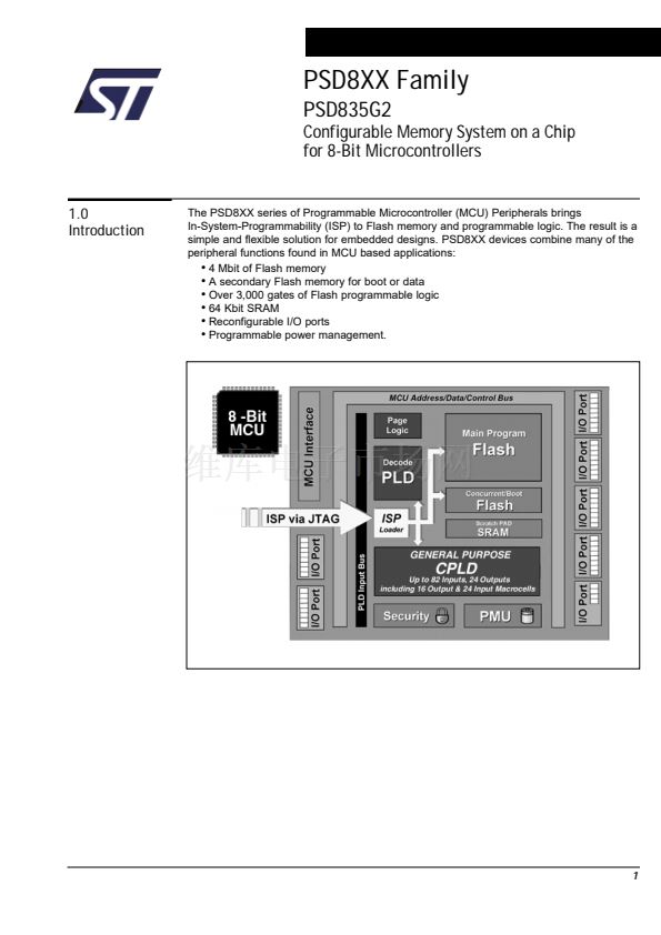
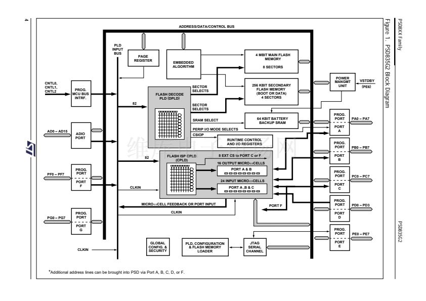
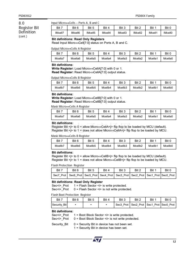
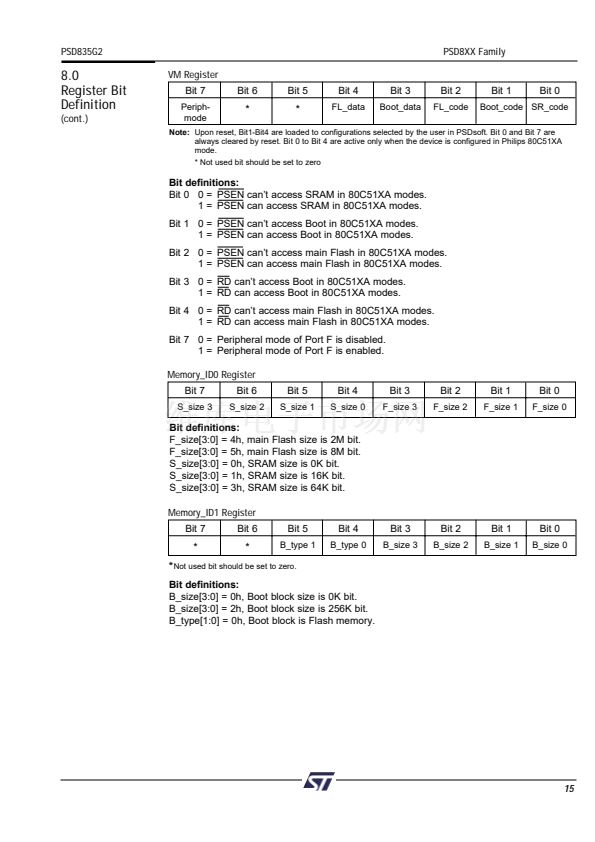
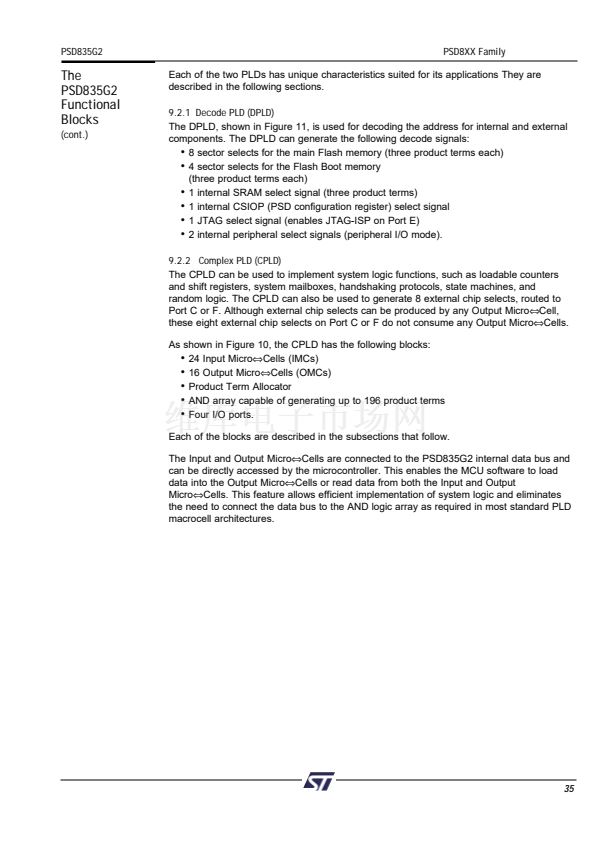
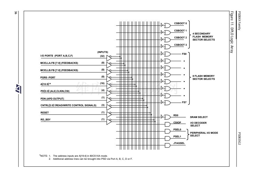
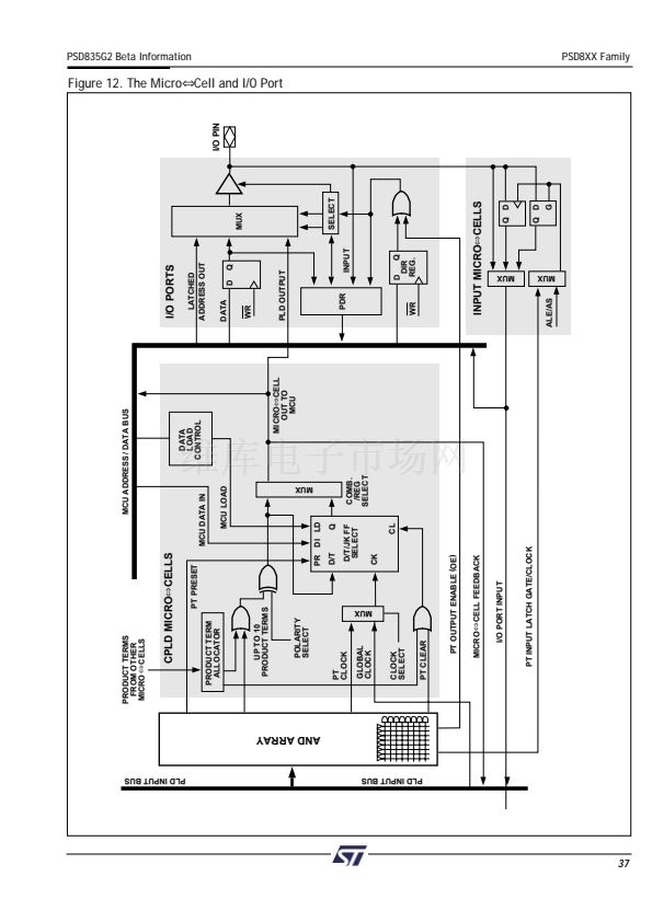
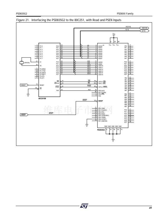
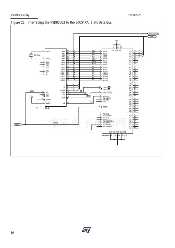
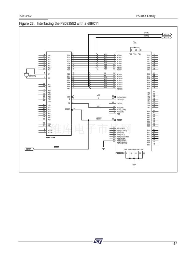
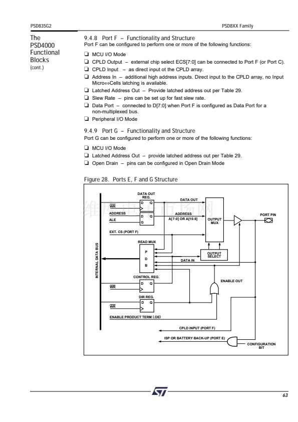
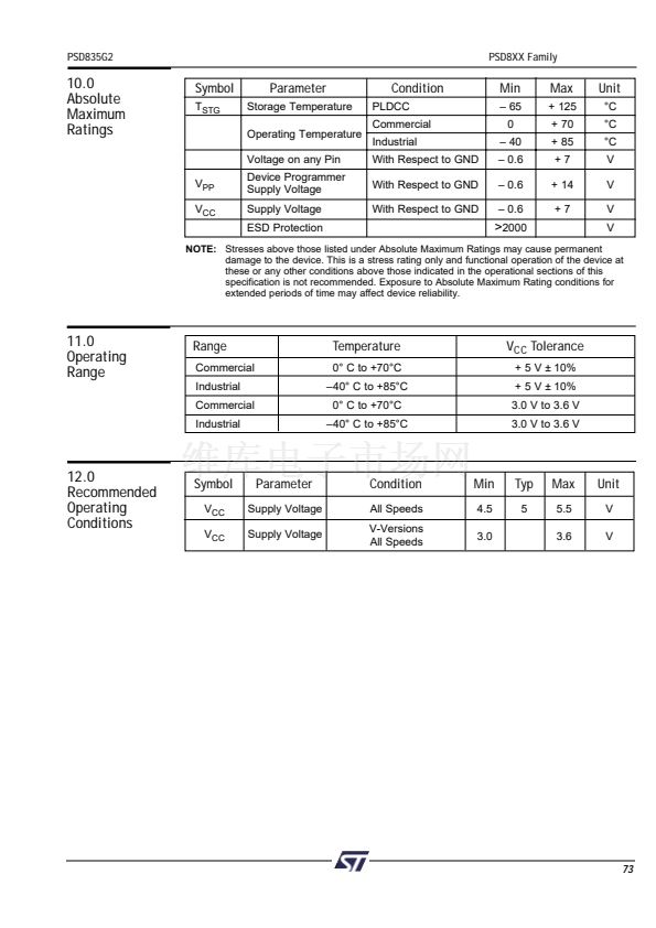
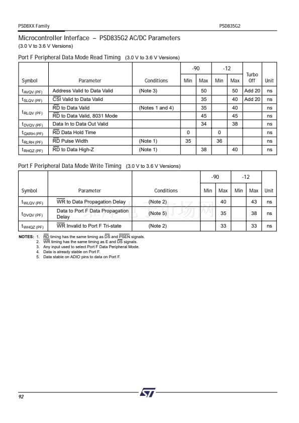
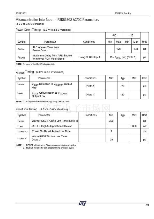
PSD8XX Family
PSD835G2
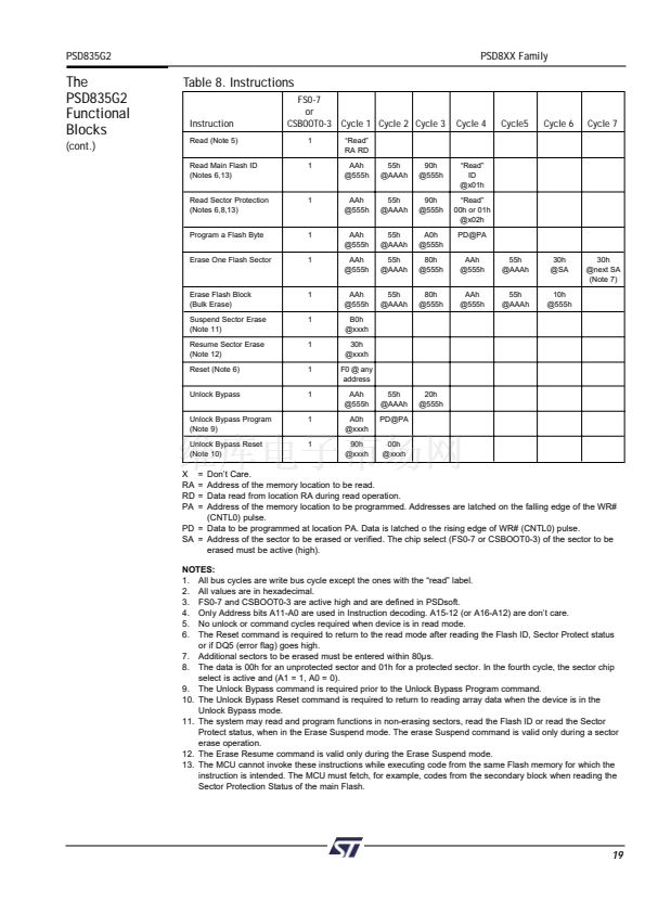
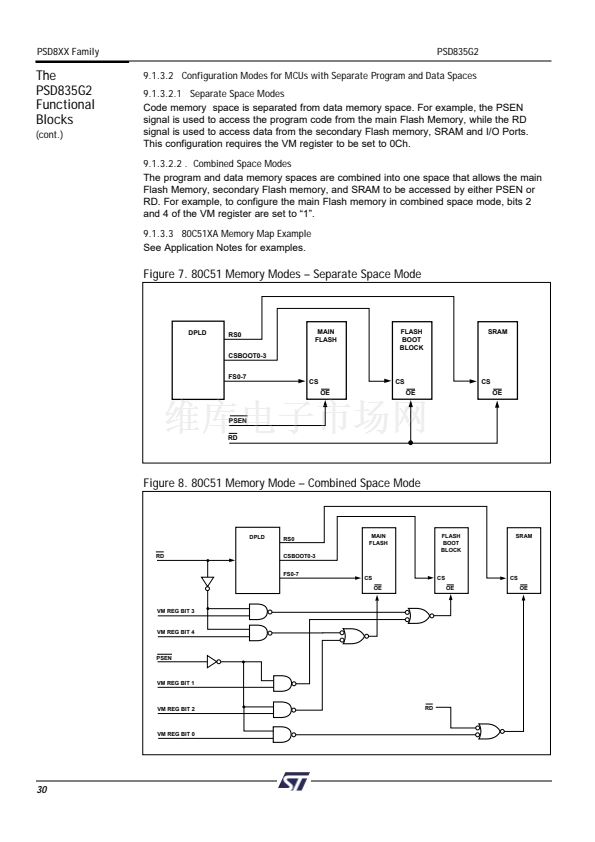
9.1.3.2 Configuration Modes for MCUs with Separate Program and Data Spaces
9.1.3.2.1 Separate Space Modes
Code memory space is separated from data memory space. For example, the PSEN
signal is used to access the program code from the main Flash Memory, while the RD
signal is used to access data from the secondary Flash memory, SRAM and I/O Ports.
This configuration requires the VM register to be set to 0Ch.
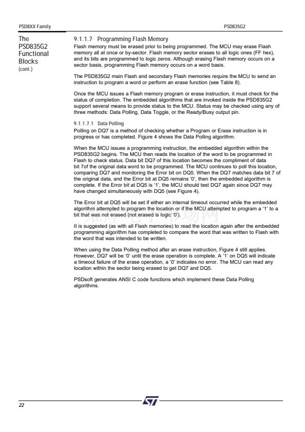
9.1.3.2.2 . Combined Space Modes
The program and data memory spaces are combined into one space that allows the main
Flash Memory, secondary Flash memory, and SRAM to be accessed by either PSEN or
RD. For example, to configure the main Flash memory in combined space mode, bits 2
and 4 of the VM register are set to 鈥?鈥?
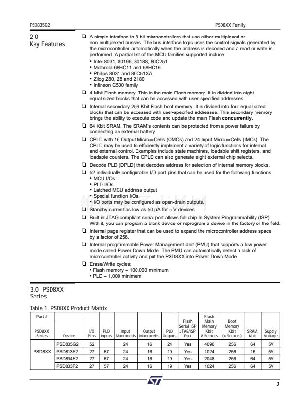
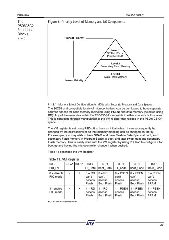
9.1.3.3 80C51XA Memory Map Example
See Application Notes for examples.
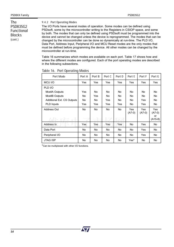
The
PSD835G2
Functional
Blocks
(cont.)
Figure 7. 80C51 Memory Modes 鈥?Separate Space Mode
DPLD
RS0
CSBOOT0-3
FS0-7
MAIN
FLASH
FLASH
BOOT
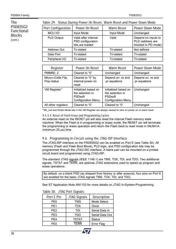
BLOCK
SRAM
CS
OE
CS
OE
CS
OE
PSEN
RD
Figure 8. 80C51 Memory Mode 鈥?Combined Space Mode
DPLD
RS0
CSBOOT0-3
FS0-7
MAIN
FLASH
FLASH
BOOT
BLOCK
SRAM
RD
CS
OE
CS
OE
CS
OE
VM REG BIT 3
VM REG BIT 4
PSEN
VM REG BIT 1
VM REG BIT 2
RD
VM REG BIT 0
30


 1
1
 2
2
 3
3
 4
4
 5
5
 6
6
 7
7
 8
8
 9
9
 10
10
 11
11
 12
12
 13
13
 14
14
 15
15
 16
16
 17
17
 18
18
 19
19
 20
20
 21
21
 22
22
 23
23
 24
24
 25
25
 26
26
 27
27
 28
28
 29
29
 30
30
 31
31
 32
32
 33
33
 34
34
 35
35
 36
36
 37
37
 38
38
 39
39
 40
40
 41
41
 42
42
 43
43
 44
44
 45
45
 46
46
 47
47
 48
48
 49
49
 50
50
 51
51
 52
52
 53
53
 54
54
 55
55
 56
56
 57
57
 58
58
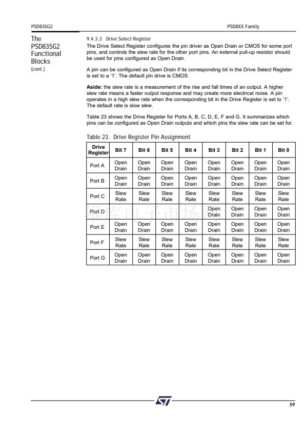
 59
59
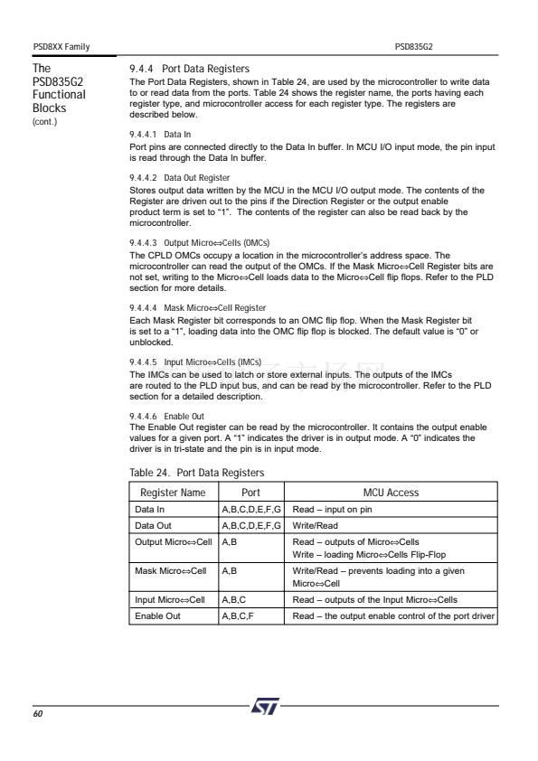
 60
60
 61
61
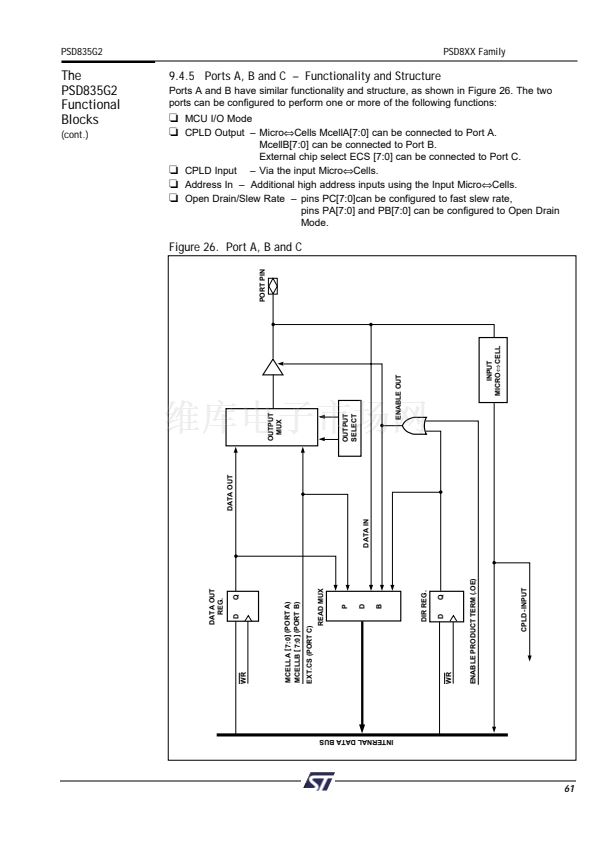 62
62
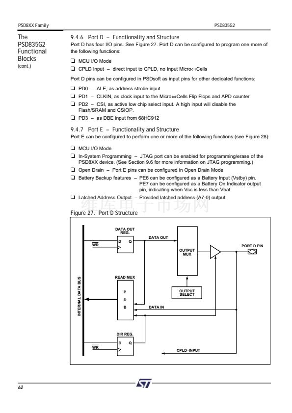 63
63
 64
64
 65
65
 66
66
 67
67
 68
68
 69
69
 70
70
 71
71
 72
72
 73
73
 74
74
 75
75
 76
76
 77
77
 78
78
 79
79
 80
80
 81
81
 82
82
 83
83
 84
84
 85
85
 86
86
 87
87
 88
88
 89
89
 90
90
 91
91
 92
92
 93
93
 94
94
 95
95
 96
96
 97
97
 98
98
 99
99
 100
100
 101
101
 102
102
 103
103
 104
104
 105
105
 106
106
 107
107
 108
108
 109
109
 110
110
