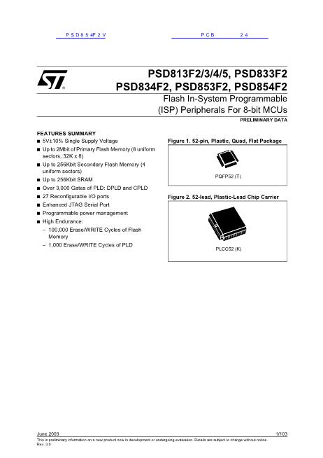
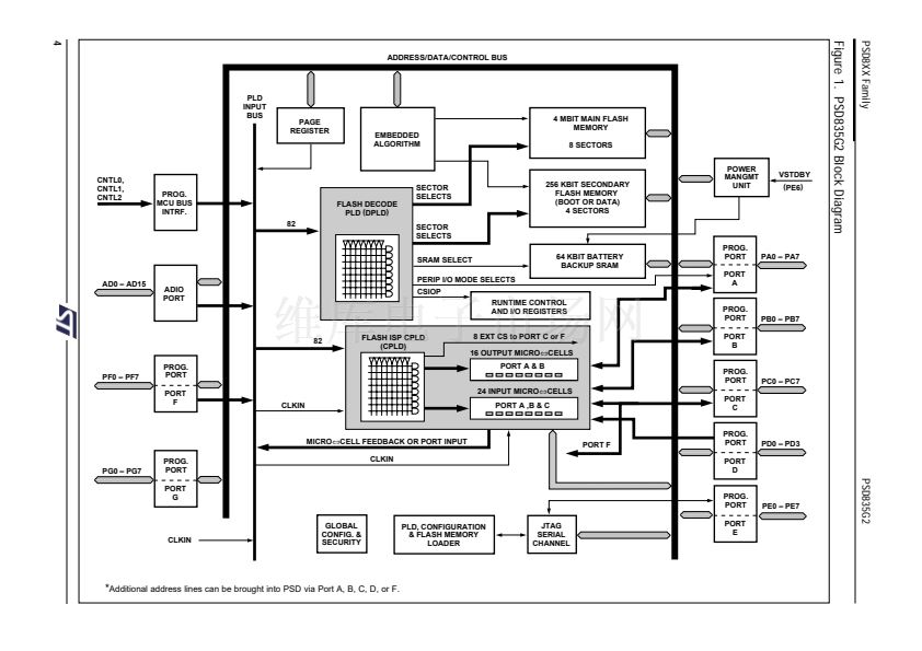
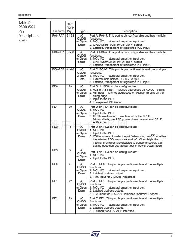
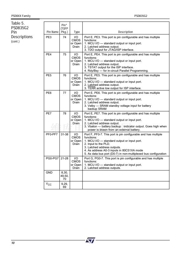
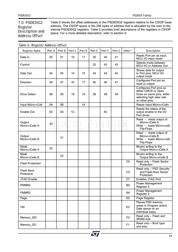
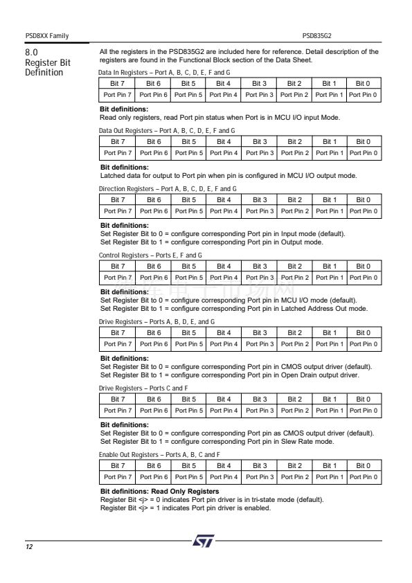
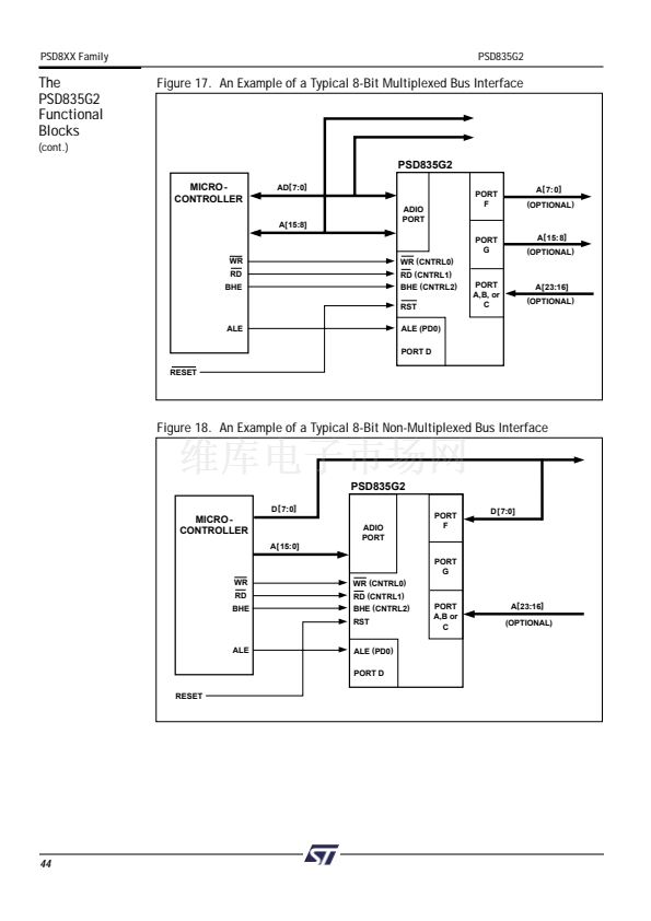
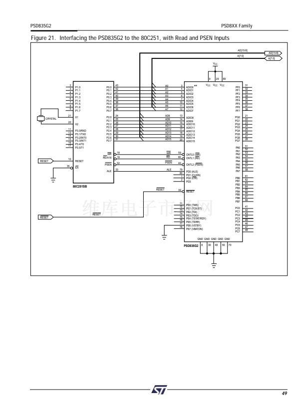
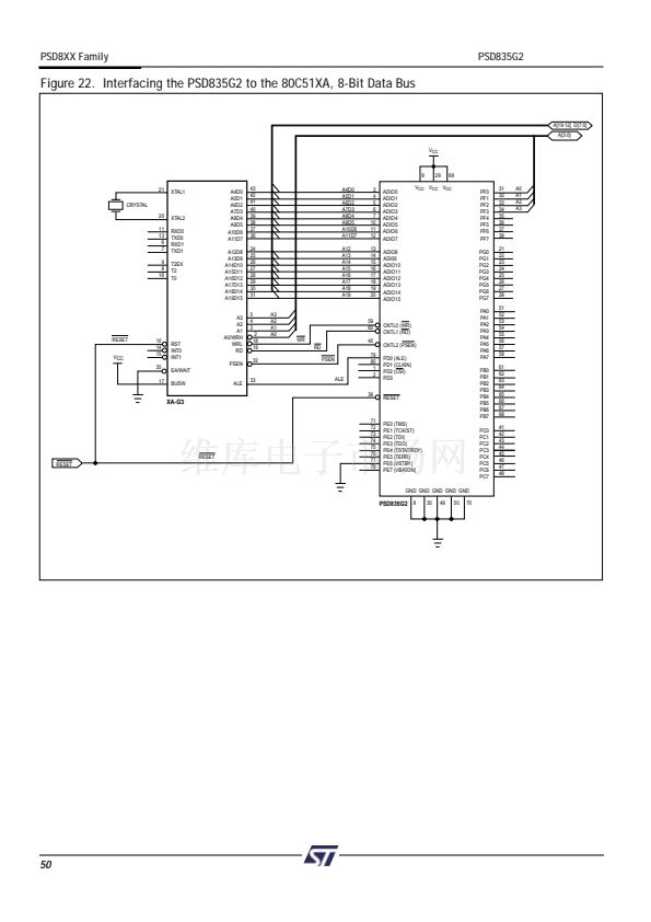
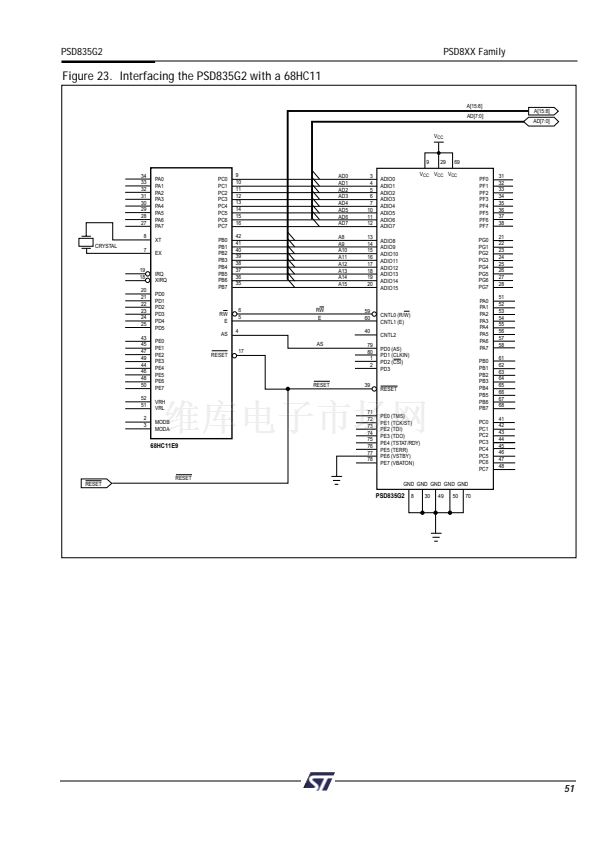
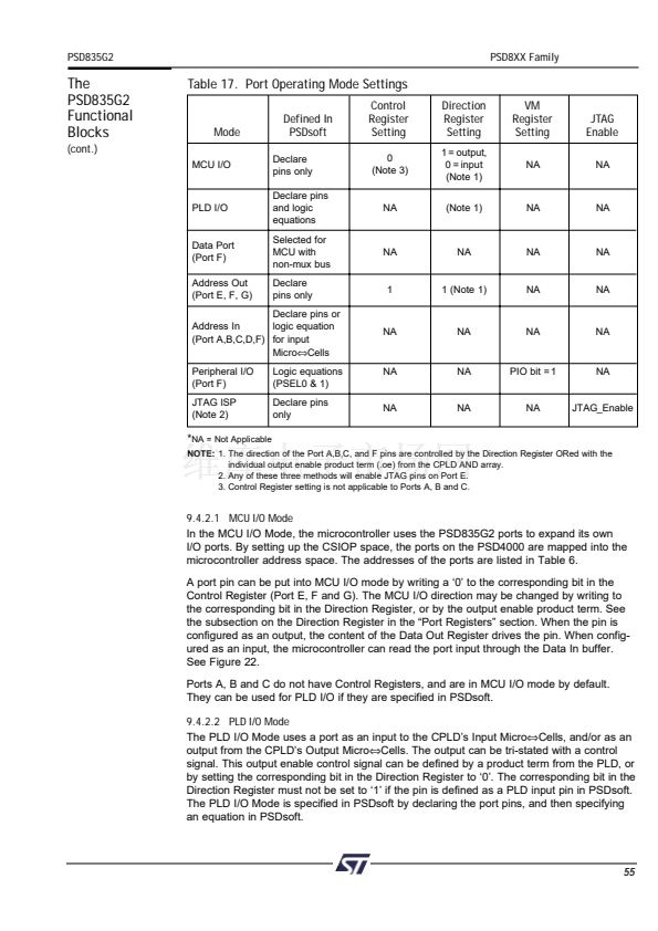
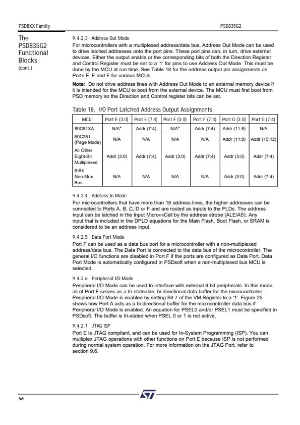
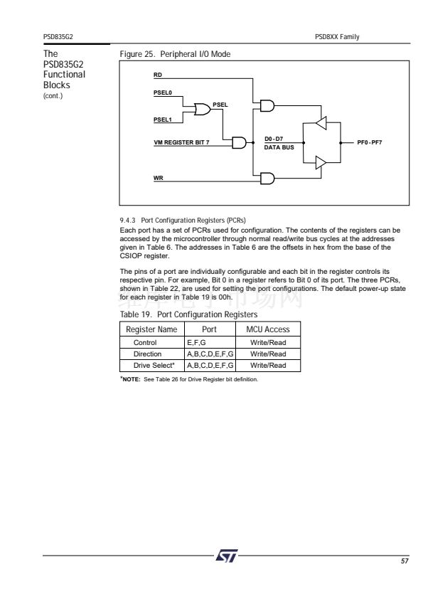
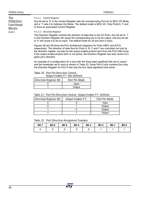
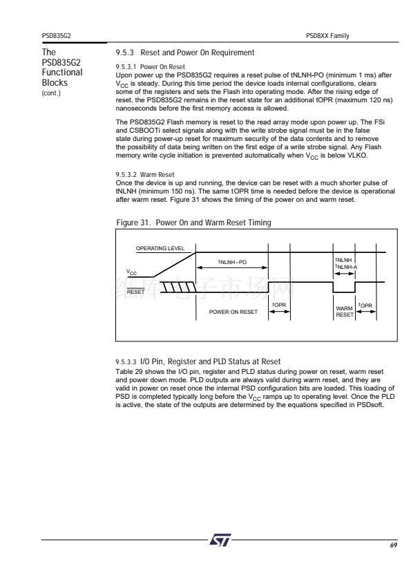
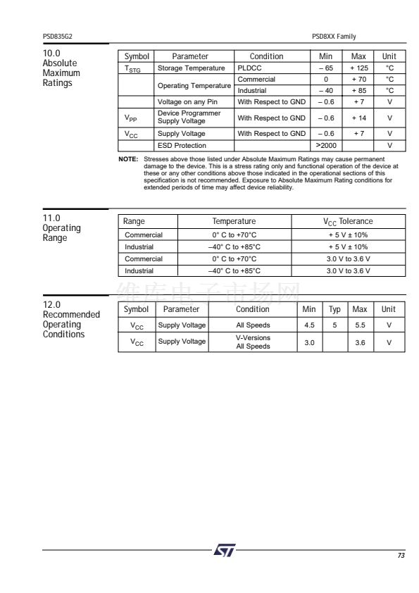
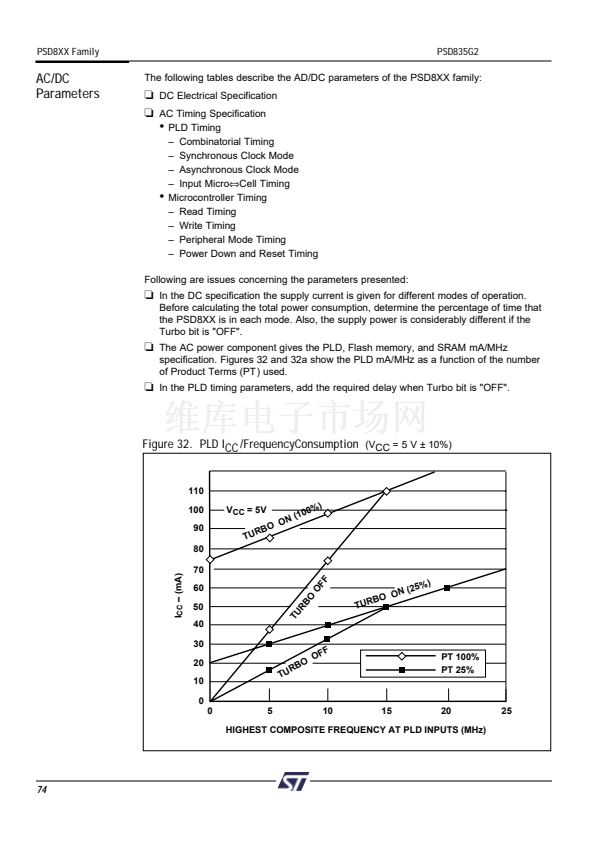
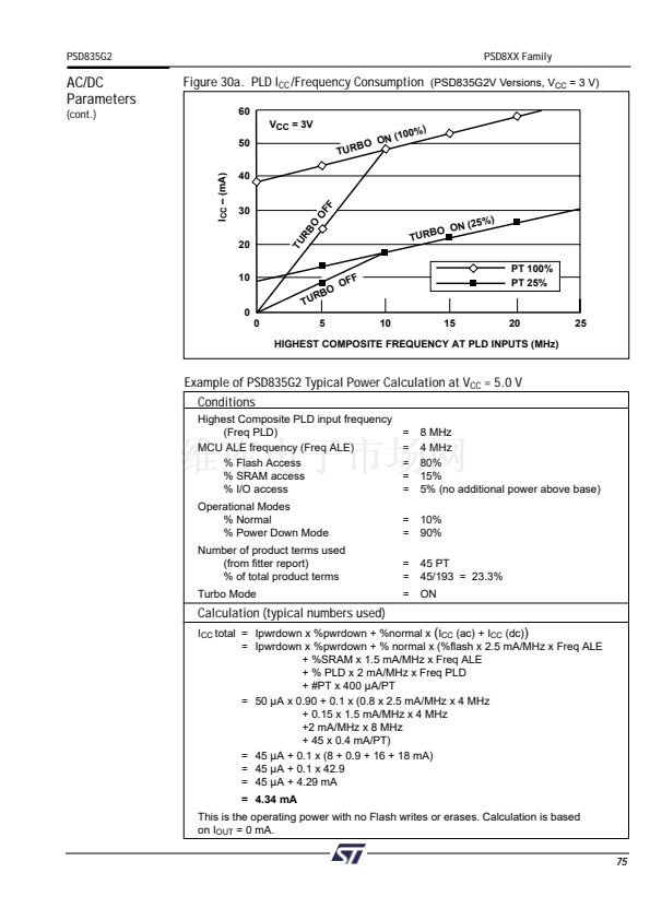
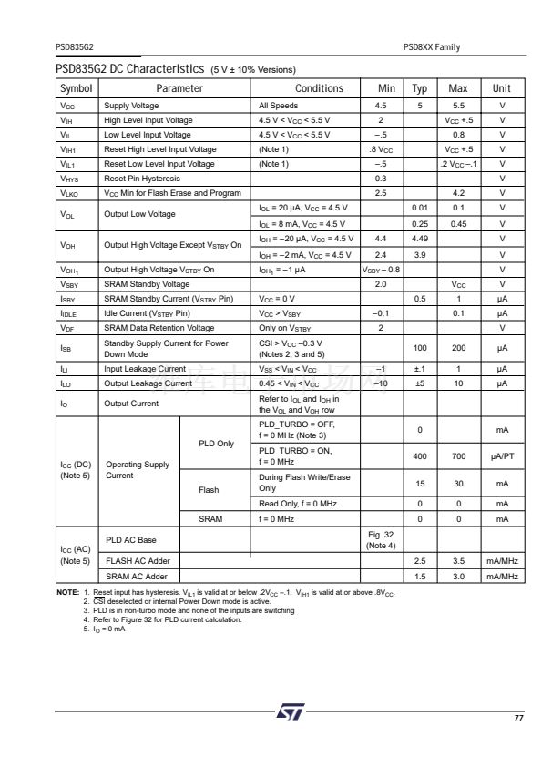
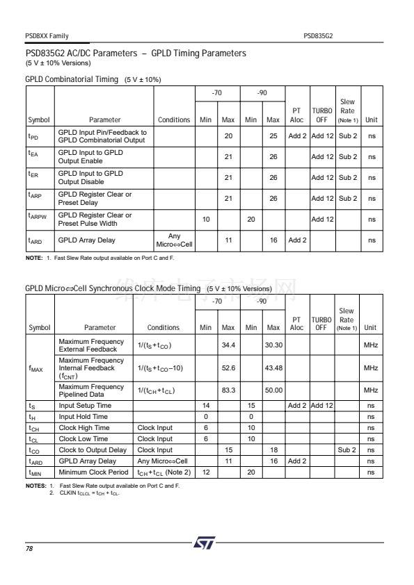
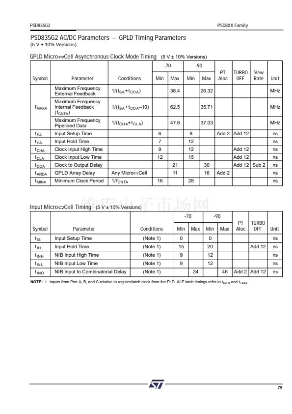
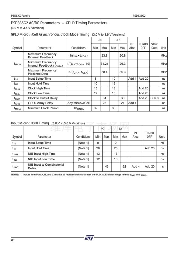
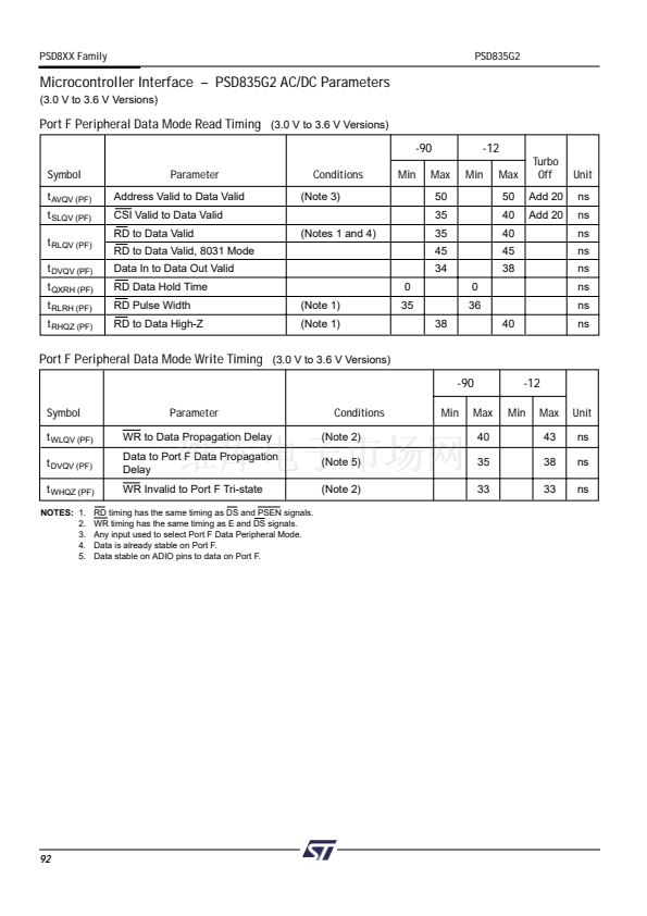
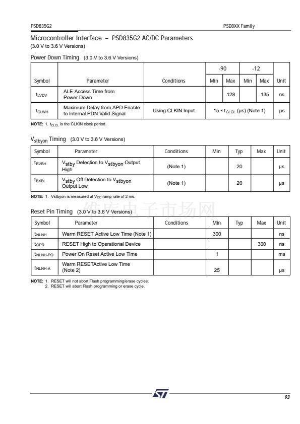
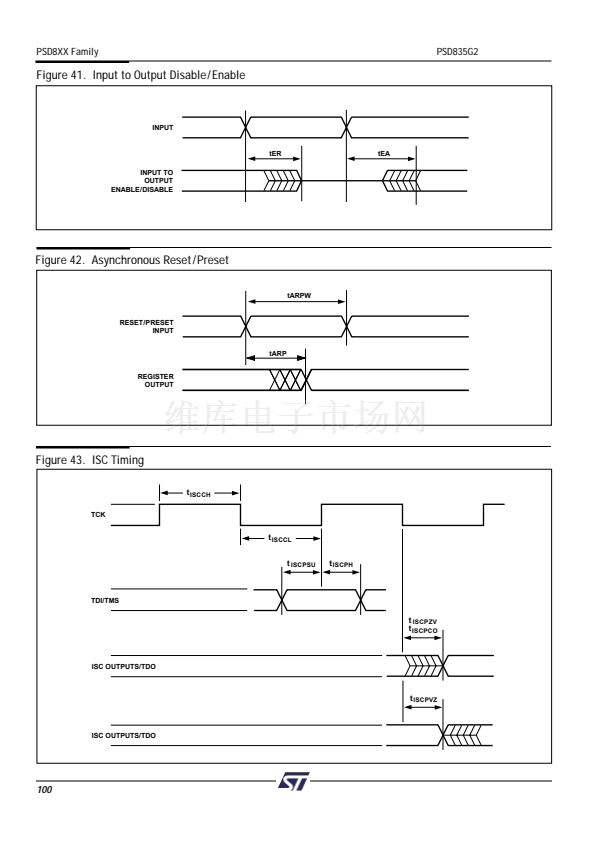
PSD835G2
PSD8XX Family
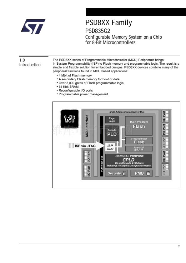
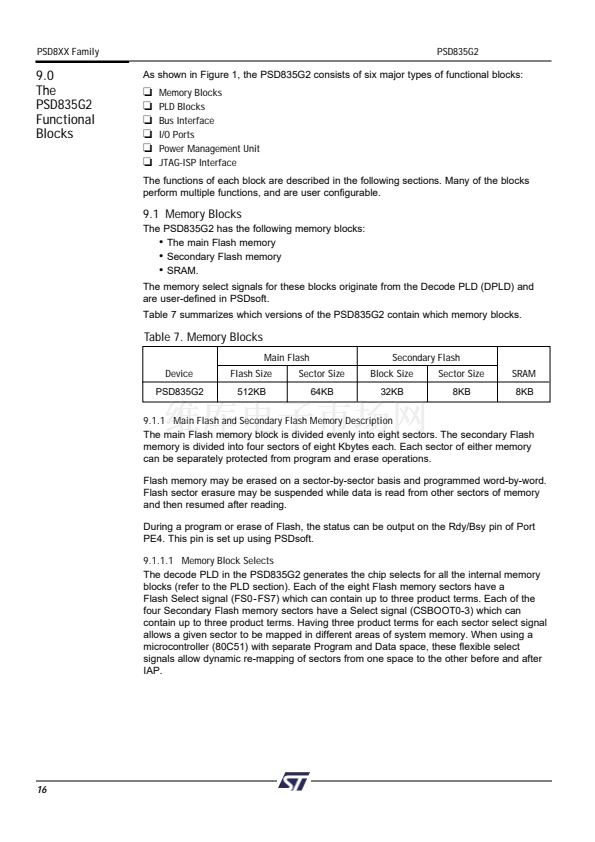
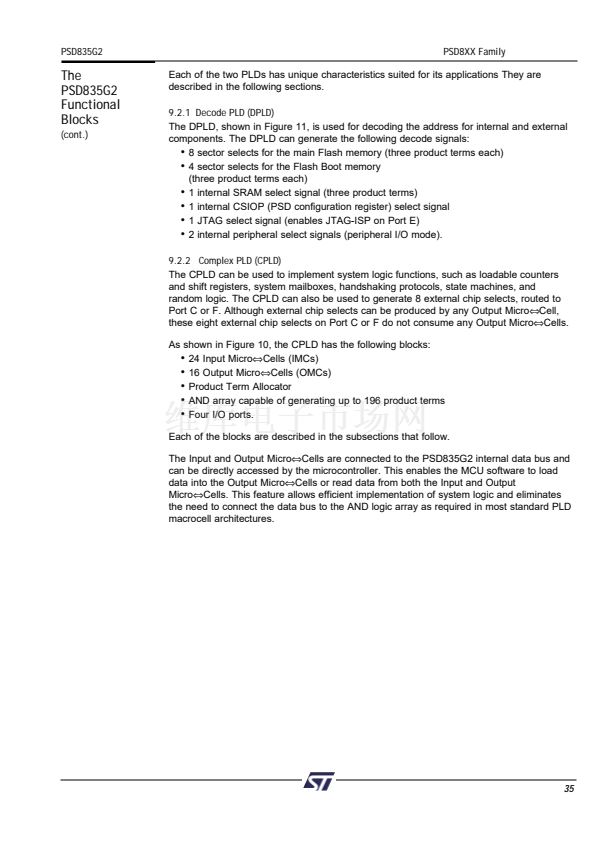
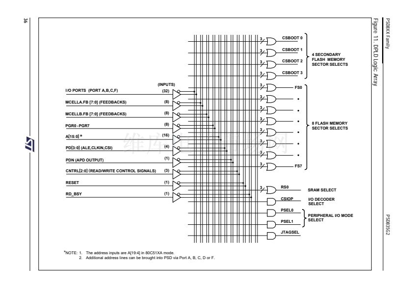
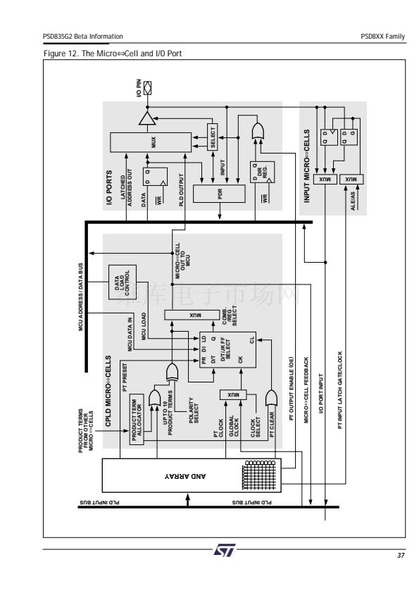
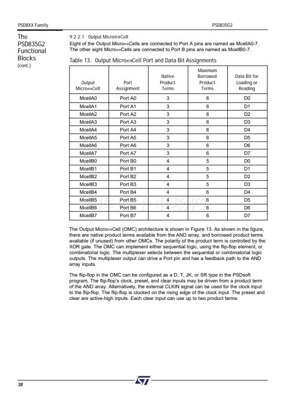
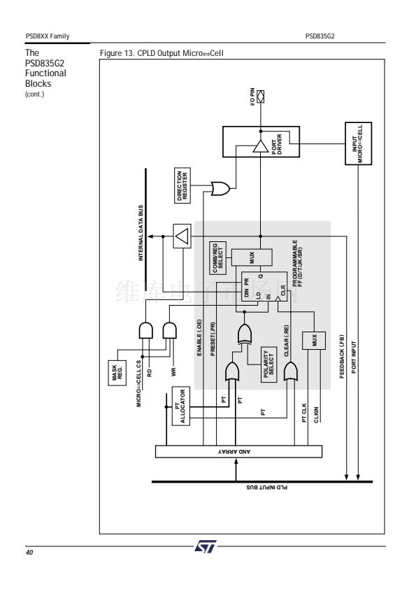
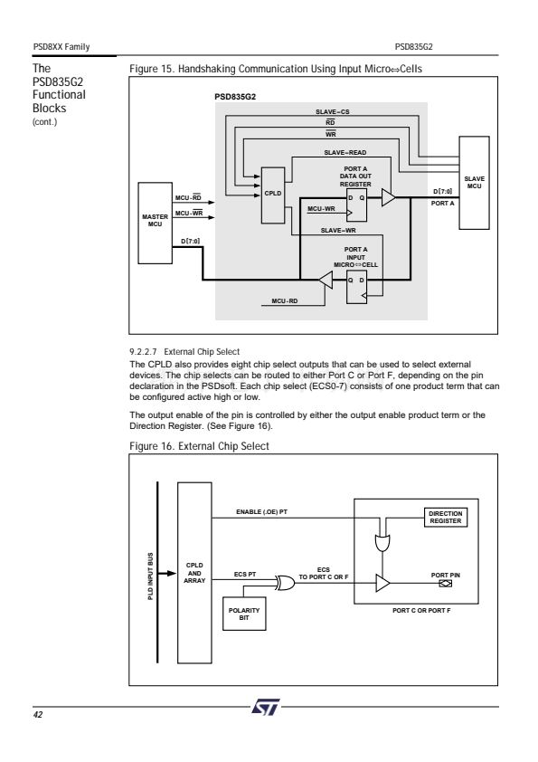
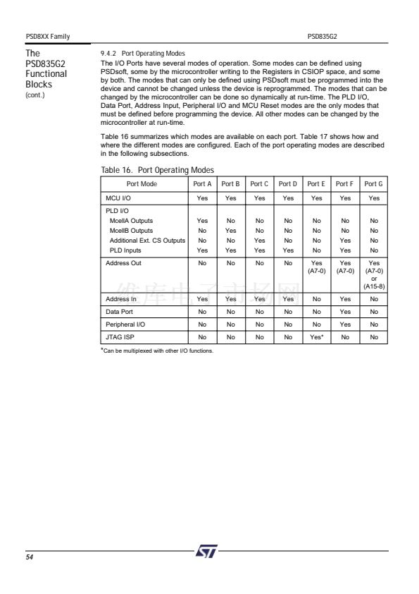
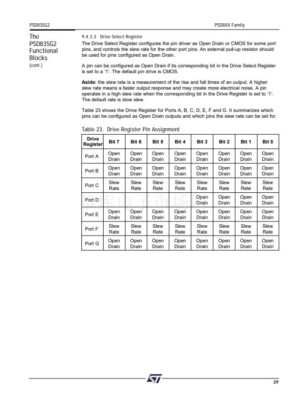
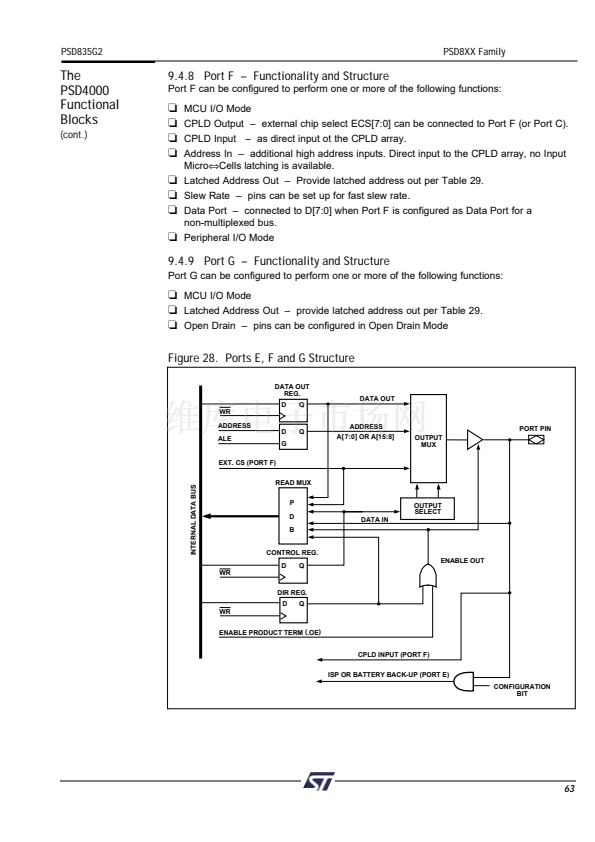
The
PSD835G2
Functional
Blocks
(cont.)
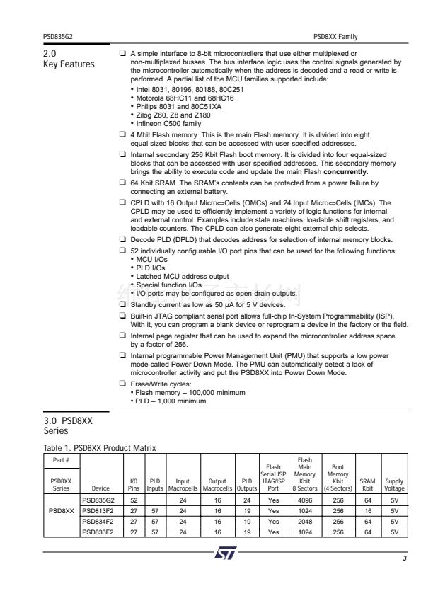
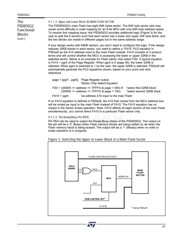
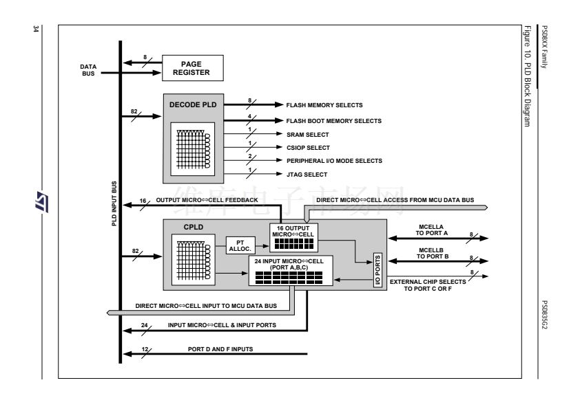
9.1.4 Page Register
The eight bit Page Register increases the addressing capability of the microcontroller by a
factor of up to 256. The contents of the register can also be read by the microcontroller.
The outputs of the Page Register (PGR0-PGR7) are inputs to the PLD decoder and
can be included in the Flash Memory, secondary Flash memory, and SRAM chip select
equations.
If memory paging is not needed, or if not all 8 page register bits are needed for memory
paging, then these bits may be used in the PLD for general logic. See Application
Notes.
Figure 9 shows the Page Register. The eight flip flops in the register are connected to the
internal data bus D0-D7. The microcontroller can write to or read from the Page Register.
The Page Register can be accessed at address location CSIOP + E0h.
Figure 9. Page Register
RESET
D0
D1
D0 - D7
D2
D3
D4
D5
D6
R/W
D7
Q0
Q1
Q2
Q3
Q4
Q5
PGR0
PGR1
PGR2
PGR3
PGR4
PGR5
PGR6
DPLD
AND
GPLD
INTERNAL
SELECTS
AND LOGIC
Q6
PGR7
Q7
PAGE
REGISTER
FLASH
PLD
31


 1
1
 2
2
 3
3
 4
4
 5
5
 6
6
 7
7
 8
8
 9
9
 10
10
 11
11
 12
12
 13
13
 14
14
 15
15
 16
16
 17
17
 18
18
 19
19
 20
20
 21
21
 22
22
 23
23
 24
24
 25
25
 26
26
 27
27
 28
28
 29
29
 30
30
 31
31
 32
32
 33
33
 34
34
 35
35
 36
36
 37
37
 38
38
 39
39
 40
40
 41
41
 42
42
 43
43
 44
44
 45
45
 46
46
 47
47
 48
48
 49
49
 50
50
 51
51
 52
52
 53
53
 54
54
 55
55
 56
56
 57
57
 58
58
 59
59
 60
60
 61
61
 62
62
 63
63
 64
64
 65
65
 66
66
 67
67
 68
68
 69
69
 70
70
 71
71
 72
72
 73
73
 74
74
 75
75
 76
76
 77
77
 78
78
 79
79
 80
80
 81
81
 82
82
 83
83
 84
84
 85
85
 86
86
 87
87
 88
88
 89
89
 90
90
 91
91
 92
92
 93
93
 94
94
 95
95
 96
96
 97
97
 98
98
 99
99
 100
100
 101
101
 102
102
 103
103
 104
104
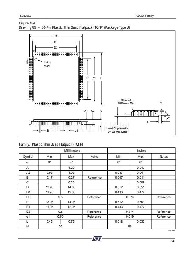
 105
105
 106
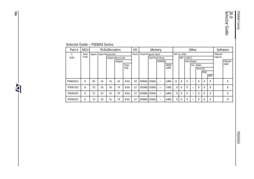
106
 107
107
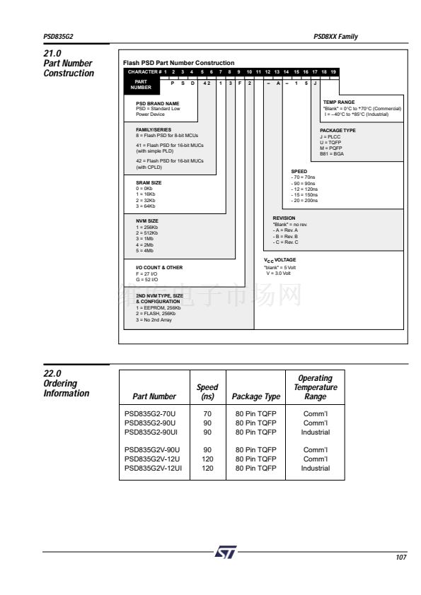 108
108
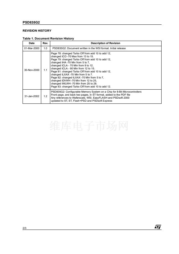 109
109
 110
110
