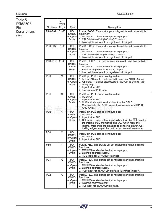
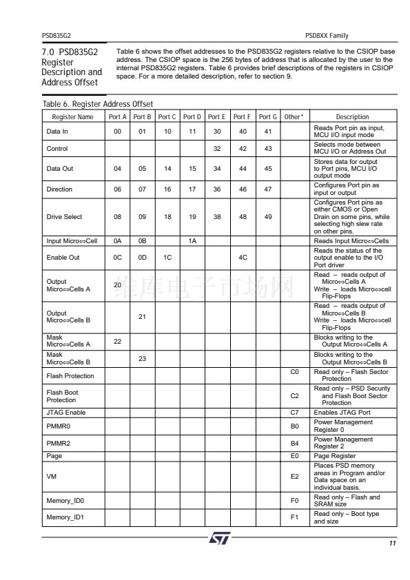
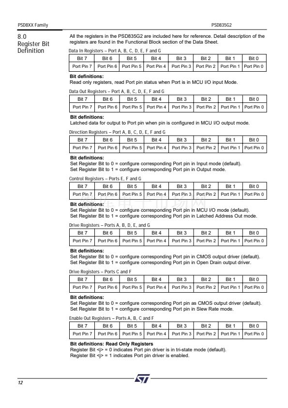
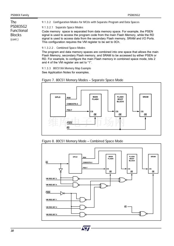
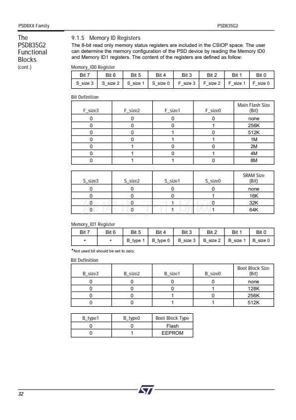
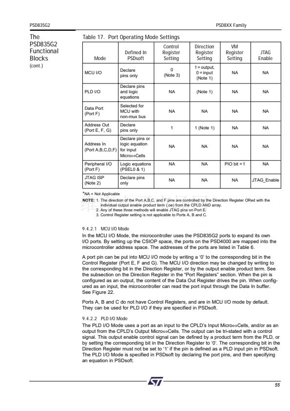
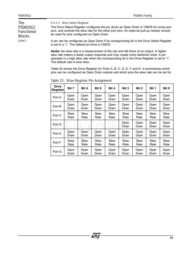
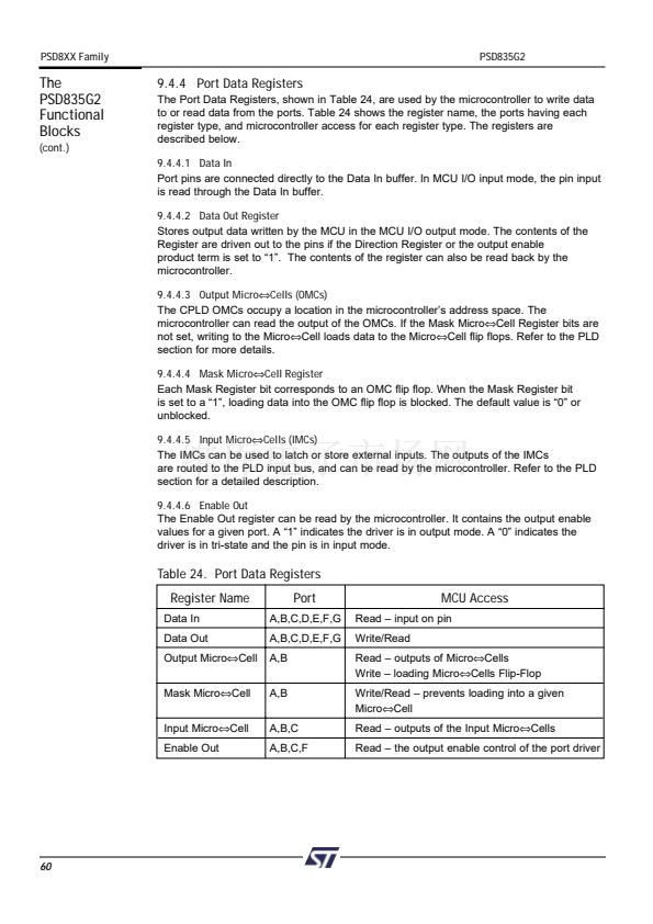
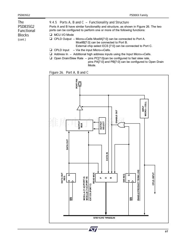
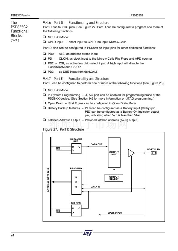
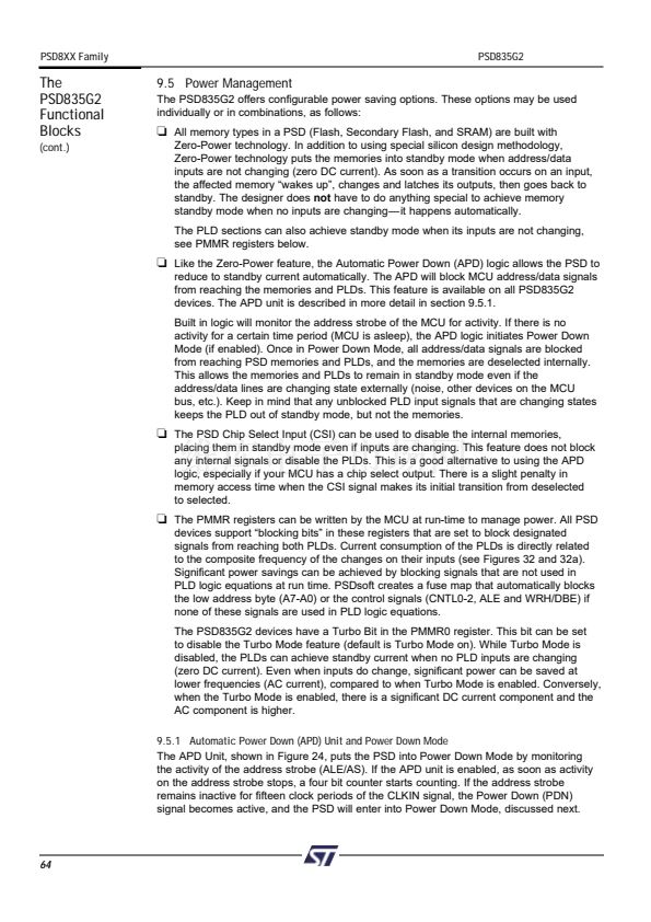
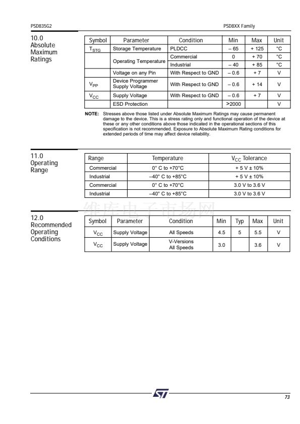
鈬?/div>
Cell
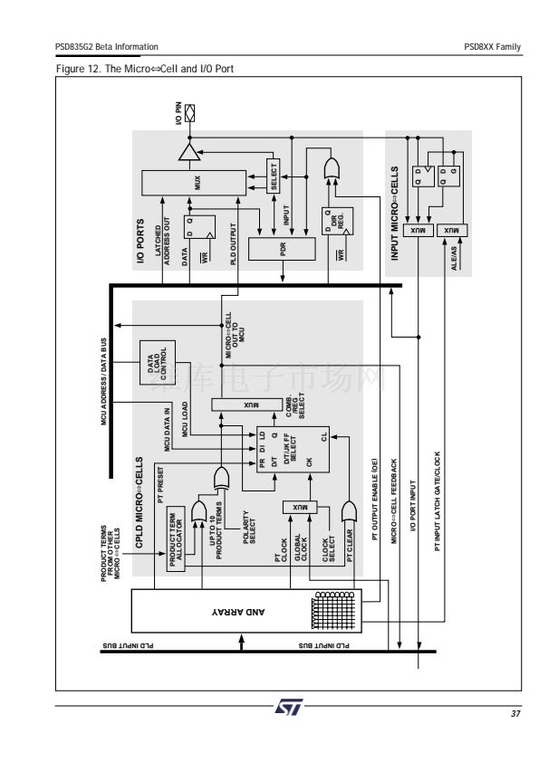
Eight of the Output Micro鈬擟ells are connected to Port A pins are named as McellA0-7.
The other eight Micro鈬擟ells are connected to Port B pins are named as McellB0-7.
The
PSD835G2
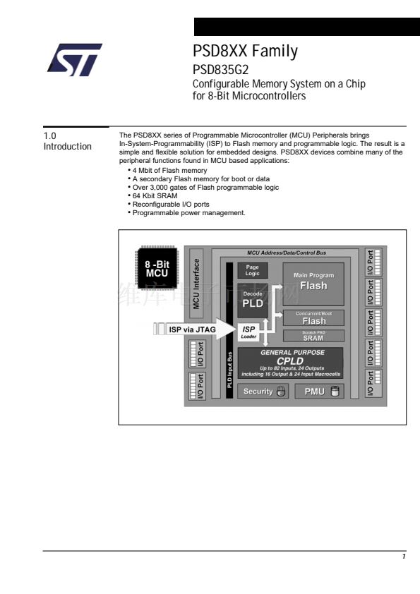
Functional
Blocks
(cont.)
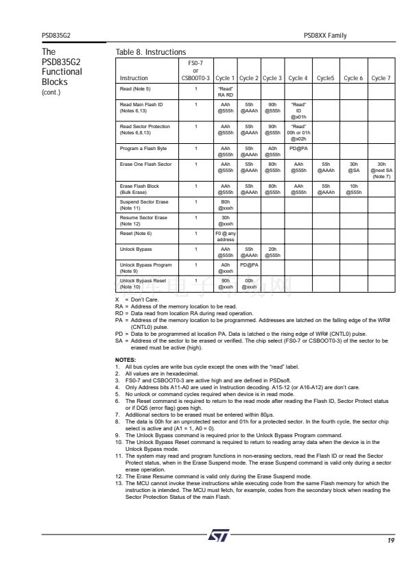
Table 13. Output Micro鈬擟ell Port and Data Bit Assignments
Native
Product
Terms
3
3
3
3
3
3
3
3
4
4
4
4
4
4
4
4
Maximum
Borrowed
Product
Terms
6
6
6
6
6
6
6
6
5
5
5
5
6
6
6
6
Data Bit for
Loading or
Reading
D0
D1
D2
D3
D4
D5
D6
D7
D0
D1
D2
D3
D4
D5
D6
D7
Output
Micro鈬擟ell
McellA0
McellA1
McellA2
McellA3
McellA4
McellA5
McellA6
McellA7
McellB0
McellB1
McellB2
McellB3
McellB4
McellB5
McellB6
McellB7
Port
Assignment
Port A0
Port A1
Port A2
Port A3
Port A4
Port A5
Port A6
Port A7
Port B0
Port B1
Port B2
Port B3
Port B4
Port B5
Port B6
Port B7
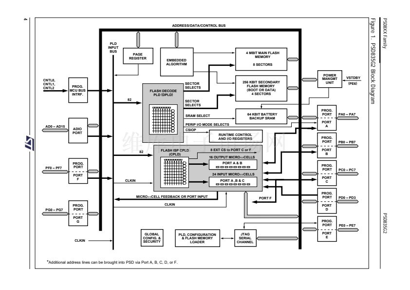
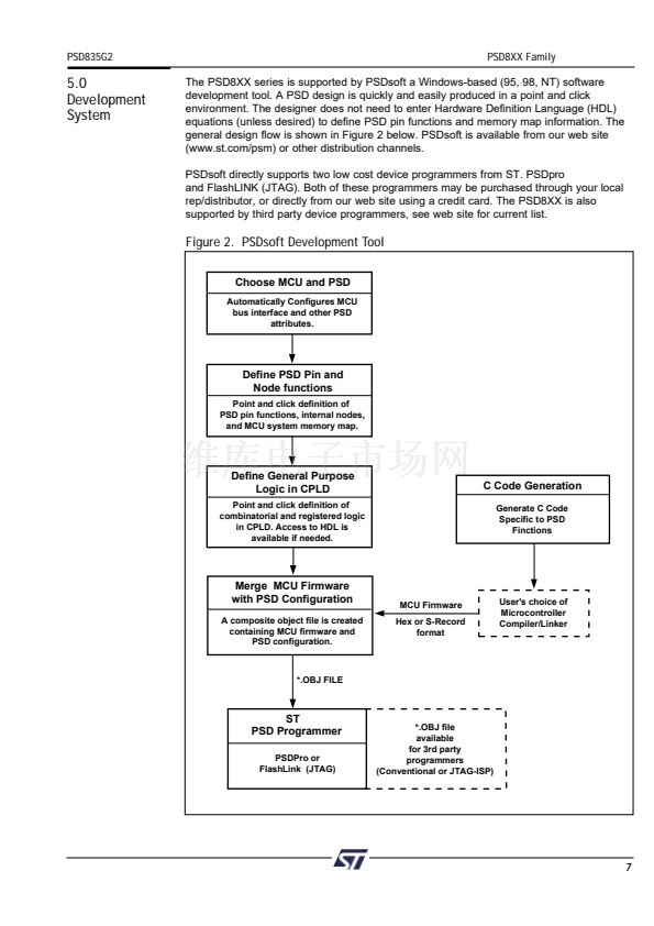
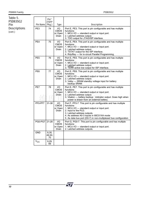
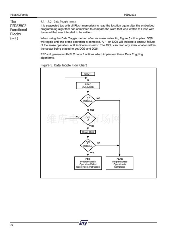
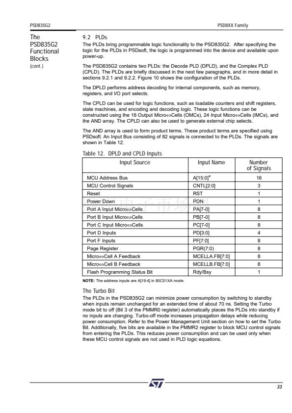
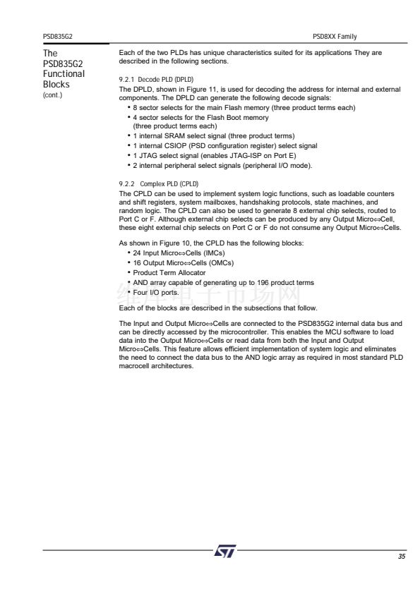
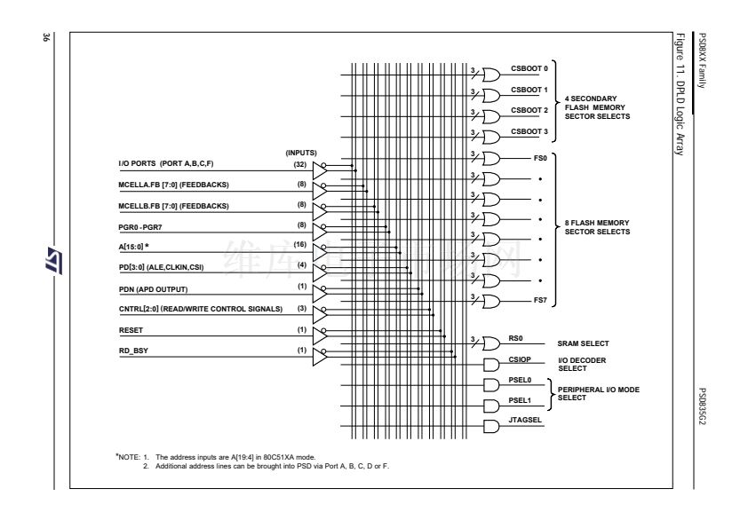
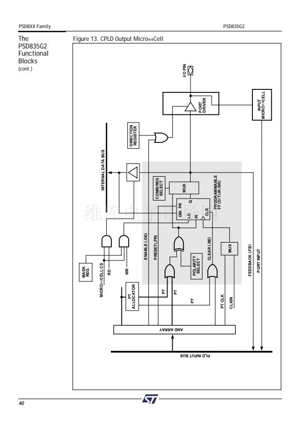
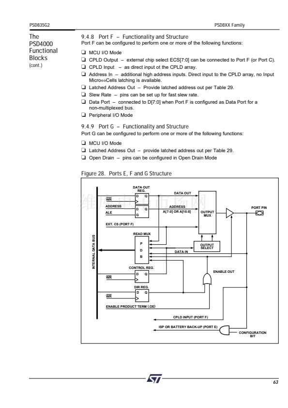
The Output Micro鈬擟ell (OMC) architecture is shown in Figure 13. As shown in the figure,
there are native product terms available from the AND array, and borrowed product terms
available (if unused) from other OMCs. The polarity of the product term is controlled by the
XOR gate. The OMC can implement either sequential logic, using the flip-flop element, or
combinatorial logic. The multiplexer selects between the sequential or combinatorial logic
outputs. The multiplexer output can drive a Port pin and has a feedback path to the AND
array inputs.
The flip-flop in the OMC can be configured as a D, T, JK, or SR type in the PSDsoft
program. The flip-flop鈥檚 clock, preset, and clear inputs may be driven from a product term
of the AND array. Alternatively, the external CLKIN signal can be used for the clock input
to the flip-flop. The flip-flop is clocked on the rising edge of the clock input. The preset and
clear are active-high inputs. Each clear input can use up to two product terms.
38


 1
1
 2
2
 3
3
 4
4
 5
5
 6
6
 7
7
 8
8
 9
9
 10
10
 11
11
 12
12
 13
13
 14
14
 15
15
 16
16
 17
17
 18
18
 19
19
 20
20
 21
21
 22
22
 23
23
 24
24
 25
25
 26
26
 27
27
 28
28
 29
29
 30
30
 31
31
 32
32
 33
33
 34
34
 35
35
 36
36
 37
37
 38
38
 39
39
 40
40
 41
41
 42
42
 43
43
 44
44
 45
45
 46
46
 47
47
 48
48
 49
49
 50
50
 51
51
 52
52
 53
53
 54
54
 55
55
 56
56
 57
57
 58
58
 59
59
 60
60
 61
61
 62
62
 63
63
 64
64
 65
65
 66
66
 67
67
 68
68
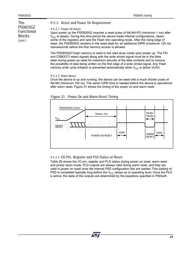
 69
69
 70
70
 71
71
 72
72
 73
73
 74
74
 75
75
 76
76
 77
77
 78
78
 79
79
 80
80
 81
81
 82
82
 83
83
 84
84
 85
85
 86
86
 87
87
 88
88
 89
89
 90
90
 91
91
 92
92
 93
93
 94
94
 95
95
 96
96
 97
97
 98
98
 99
99
 100
100
 101
101
 102
102
 103
103
 104
104
 105
105
 106
106
 107
107
 108
108
 109
109
 110
110
