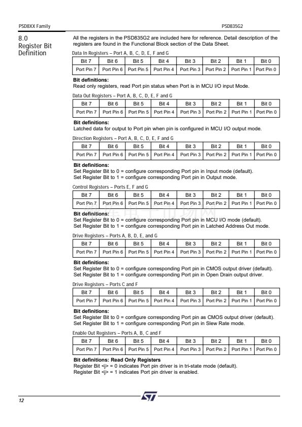
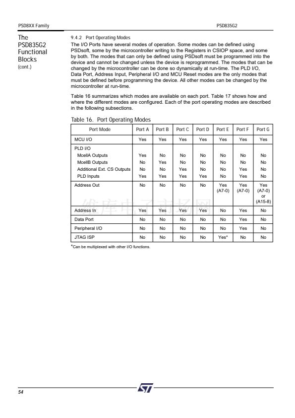
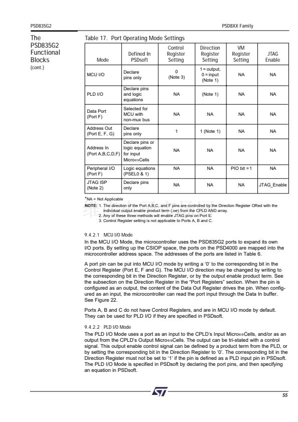
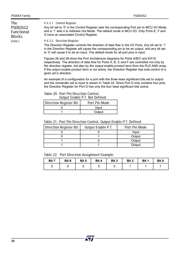
Any bit set to 鈥?鈥?in the Control Register sets the corresponding Port pin to MCU I/O Mode,
and a 鈥?鈥?sets it to Address Out Mode. The default mode is MCU I/O. Only Ports E, F and
G have an associated Control Register.
The Direction Register controls the direction of data flow in the I/O Ports. Any bit set to 鈥?鈥?/div>
in the Direction Register will cause the corresponding pin to be an output, and any bit set
to 鈥?鈥?will cause it to be an input. The default mode for all port pins is input.
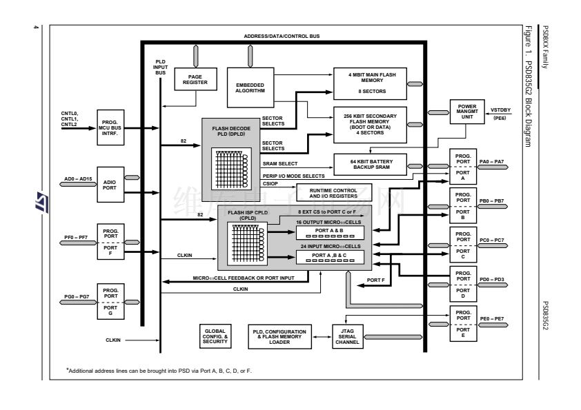
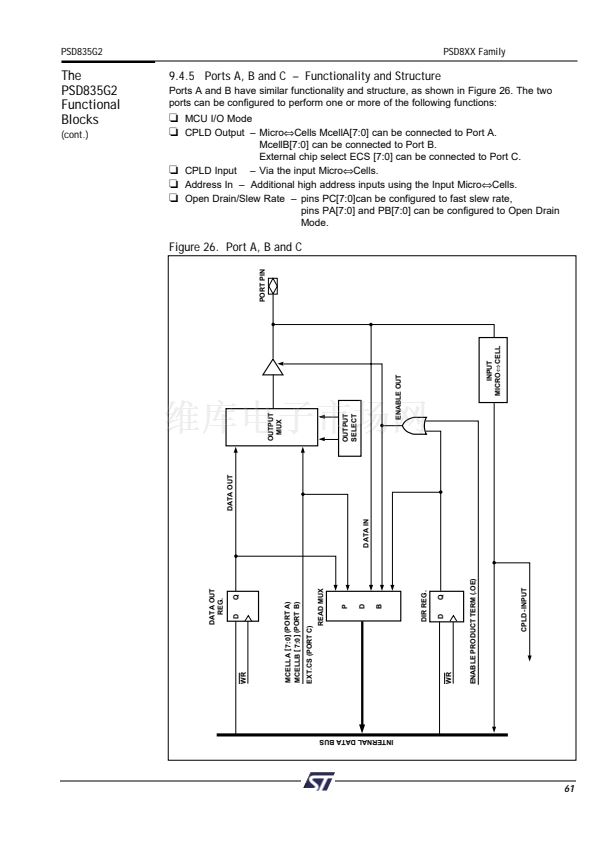
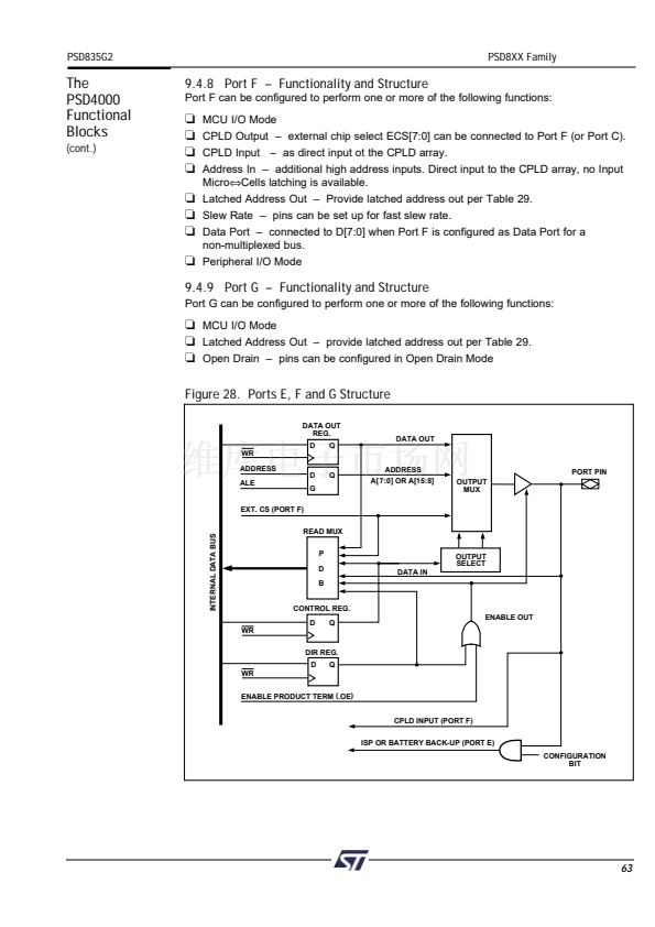
Figures 26 and 28 show the Port Architecture diagrams for Ports A/B/C and E/F/G
respectively. The direction of data flow for Ports A, B, C and F are controlled not only by
the direction register, but also by the output enable product term from the PLD AND array.
If the output enable product term is not active, the Direction Register has sole control of a
given pin鈥檚 direction.
An example of a configuration for a port with the three least significant bits set to output
and the remainder set to input is shown in Table 22. Since Port D only contains four pins,
the Direction Register for Port D has only the four least significant bits active.
The
PSD835G2
Functional
Blocks
(cont.)
Table 20. Port Pin Direction Control,
Output Enable P.T. Not Defined
Direction Register Bit
Port Pin Mode
0
1
Input
Output
Table 21. Port Pin Direction Control, Output Enable P.T. Defined
Direction Register Bit
Output Enable P.T.
Port Pin Mode
0
0
1
1
0
1
0
1
Input
Output
Output
Output
Table 22. Port Direction Assignment Example
Bit 7
0
Bit 6
0
Bit 5
0
Bit 4
0
Bit 3
0
Bit 2
1
Bit 1
1
Bit 0
1
58


 1
1
 2
2
 3
3
 4
4
 5
5
 6
6
 7
7
 8
8
 9
9
 10
10
 11
11
 12
12
 13
13
 14
14
 15
15
 16
16
 17
17
 18
18
 19
19
 20
20
 21
21
 22
22
 23
23
 24
24
 25
25
 26
26
 27
27
 28
28
 29
29
 30
30
 31
31
 32
32
 33
33
 34
34
 35
35
 36
36
 37
37
 38
38
 39
39
 40
40
 41
41
 42
42
 43
43
 44
44
 45
45
 46
46
 47
47
 48
48
 49
49
 50
50
 51
51
 52
52
 53
53
 54
54
 55
55
 56
56
 57
57
 58
58
 59
59
 60
60
 61
61
 62
62
 63
63
 64
64
 65
65
 66
66
 67
67
 68
68
 69
69
 70
70
 71
71
 72
72
 73
73
 74
74
 75
75
 76
76
 77
77
 78
78
 79
79
 80
80
 81
81
 82
82
 83
83
 84
84
 85
85
 86
86
 87
87
 88
88
 89
89
 90
90
 91
91
 92
92
 93
93
 94
94
 95
95
 96
96
 97
97
 98
98
 99
99
 100
100
 101
101
 102
102
 103
103
 104
104
 105
105
 106
106
 107
107
 108
108
 109
109
 110
110
