PSD835G2
PSD8XX Family
The
PSD835G2
Functional
Blocks
(cont.)
9.4.5 Ports A, B and C 鈥?Functionality and Structure
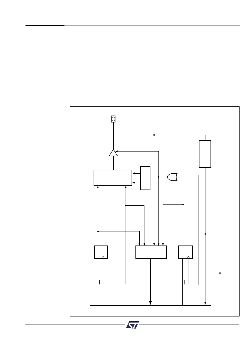
Ports A and B have similar functionality and structure, as shown in Figure 26. The two
ports can be configured to perform one or more of the following functions:
t
MCU I/O Mode
t
CPLD Output 鈥?Micro鈬擟ells McellA[7:0] can be connected to Port A.
McellB[7:0] can be connected to Port B.
External chip select ECS [7:0] can be connected to Port C.
t
CPLD Input 鈥?Via the input Micro鈬擟ells.
t
Address In 鈥?Additional high address inputs using the Input Micro鈬擟ells.
t
Open Drain/Slew Rate 鈥?pins PC[7:0]can be configured to fast slew rate,
pins PA[7:0] and PB[7:0] can be configured to Open Drain
Mode.
Figure 26. Port A, B and C
PORT PIN
OUTPUT
MUX
DATA OUT
OUTPUT
SELECT
DATA IN
ENABLE OUT
ENABLE PRODUCT TERM (.OE)
INPUT
MICRO
鈬?/div>
CELL
MCELLA [ 7:0 ] (PORT A)
MCELLB [ 7:0 ] (PORT B)
WR
EXT.CS (PORT C)
WR
CPLD -INPUT
READ MUX
DATA OUT
REG.
DIR REG.
Q
D
D
B
P
D
Q
INTERNAL DATA BUS
61
