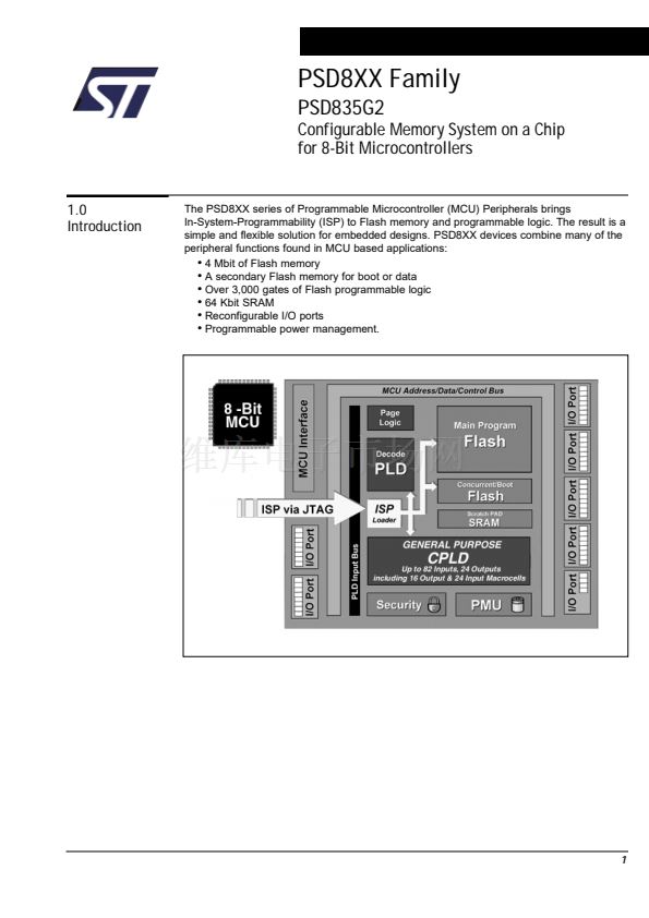
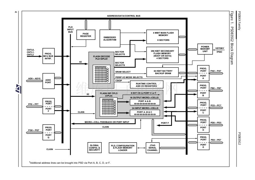
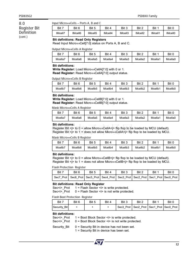
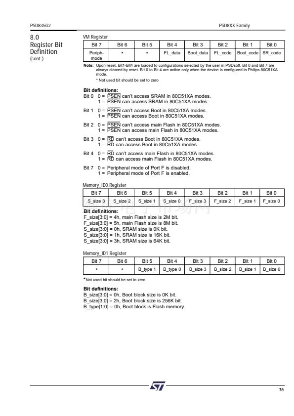
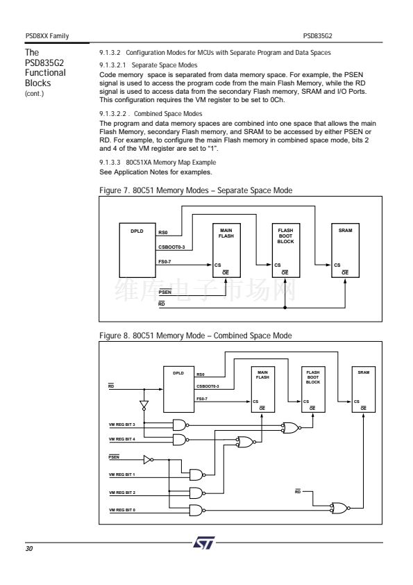
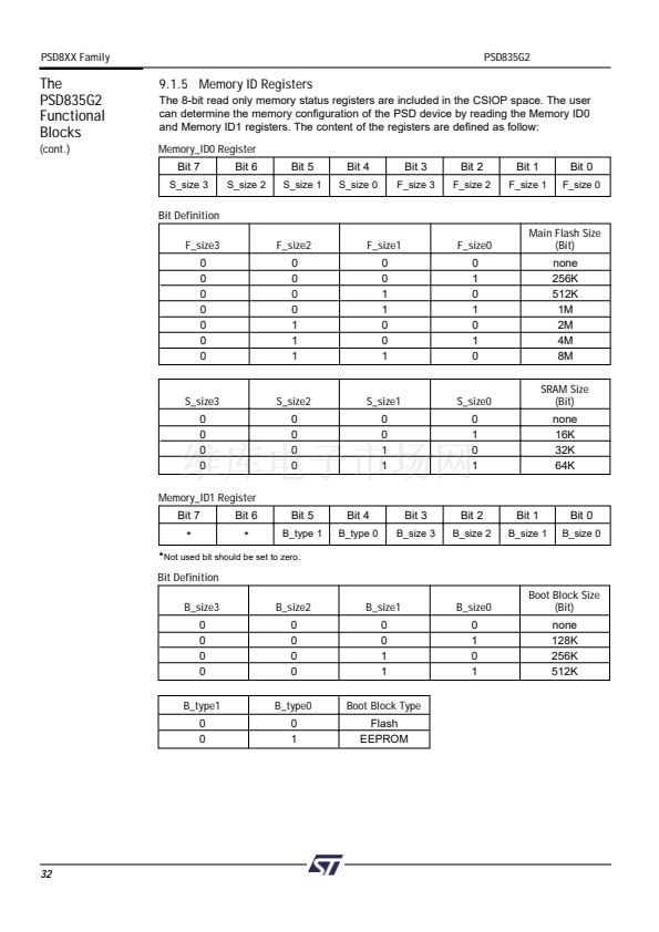
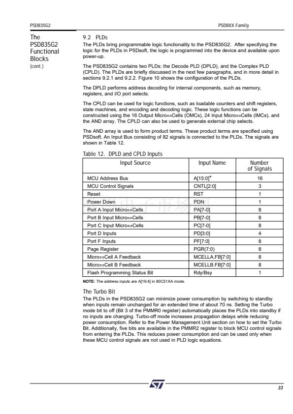
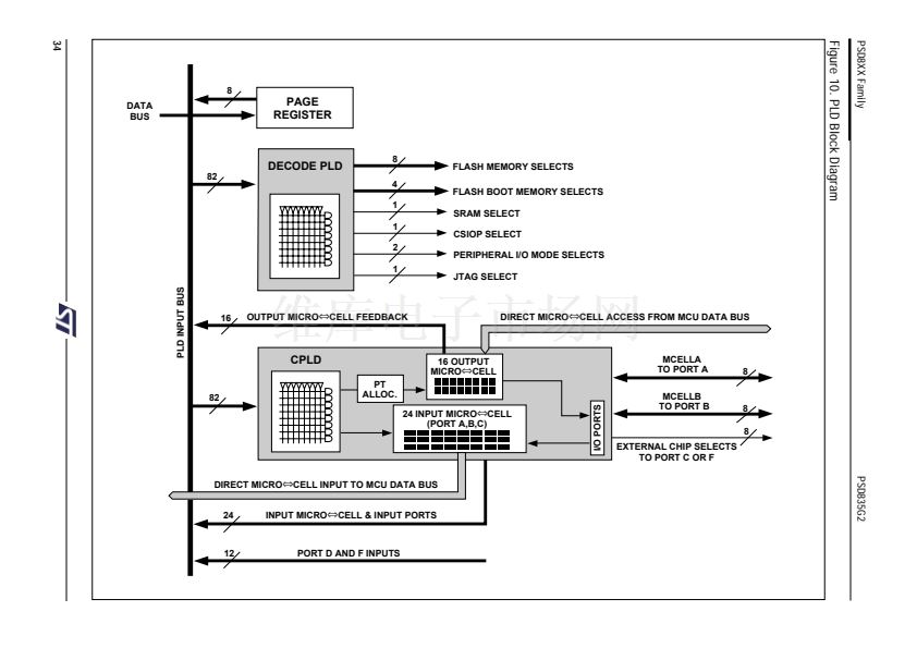
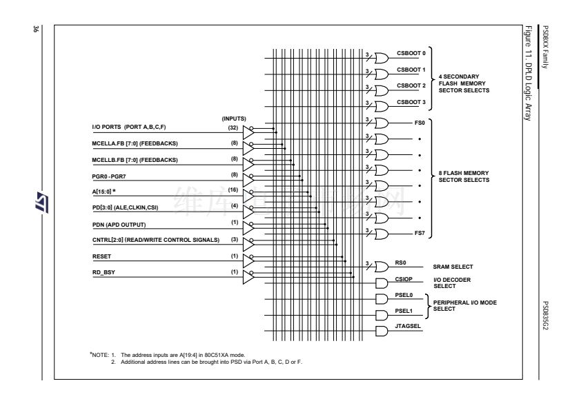
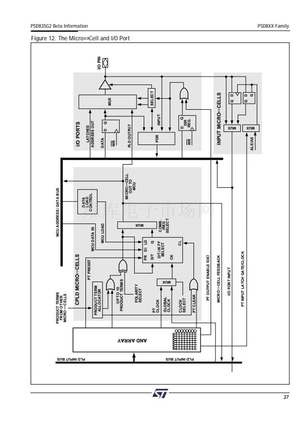
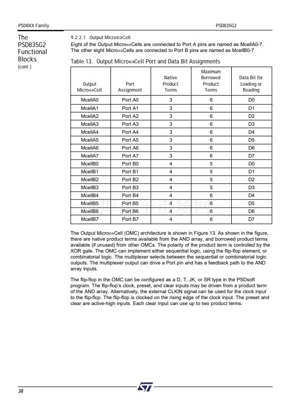
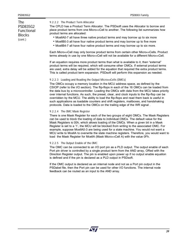
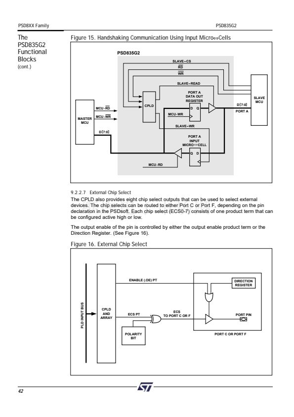
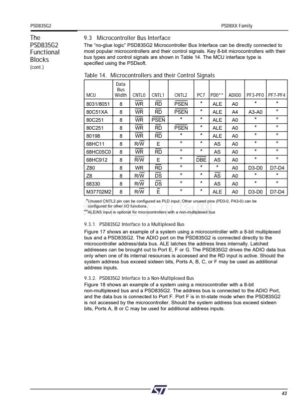
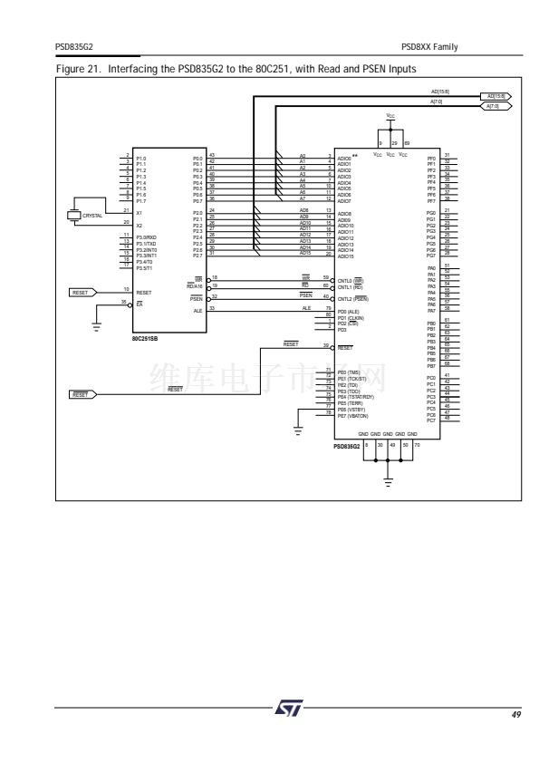
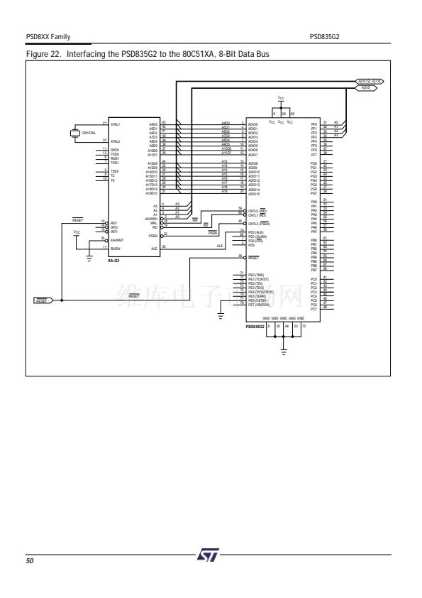
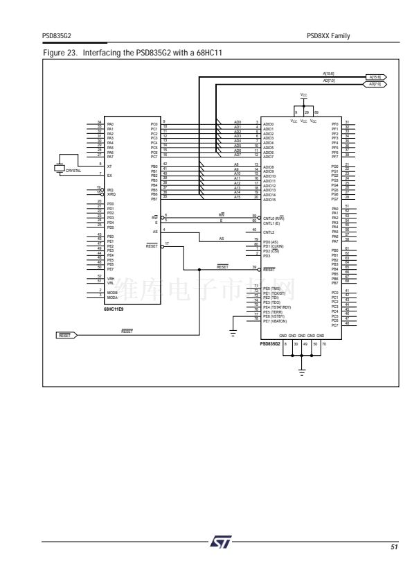
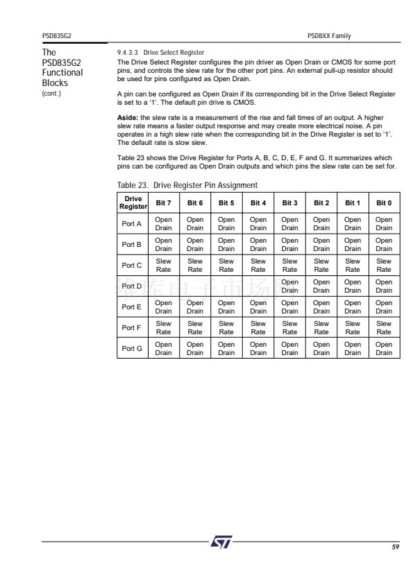
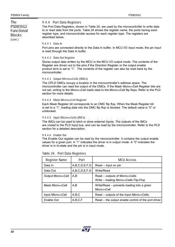
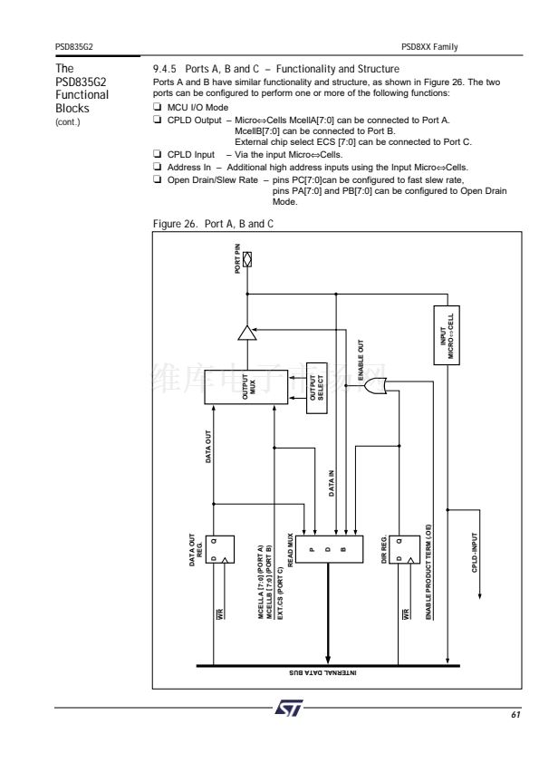
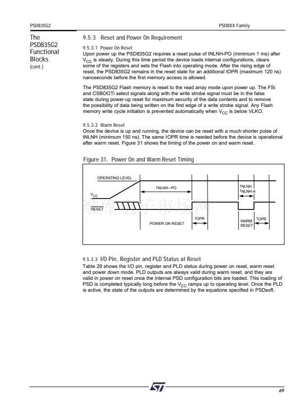
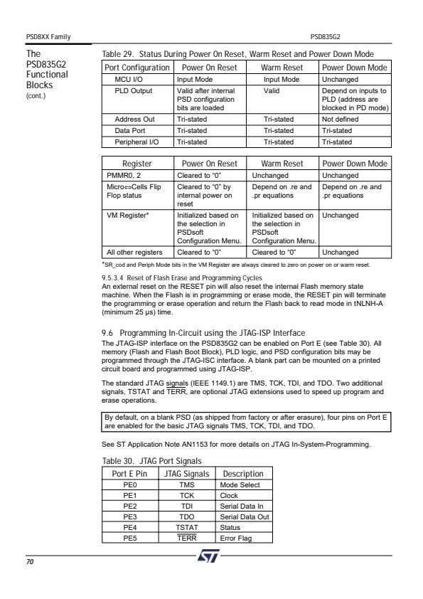
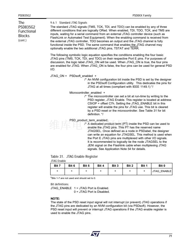
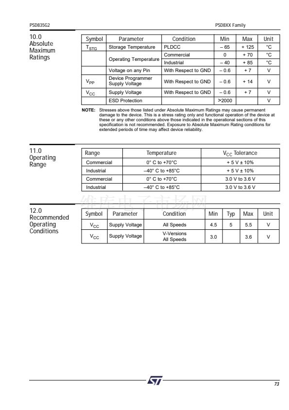
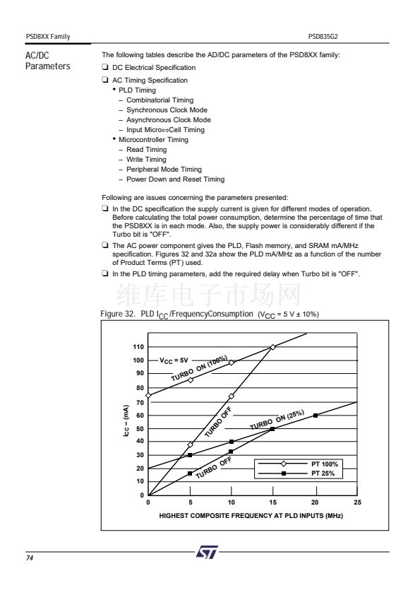
PSD8XX Family
PSD835G2
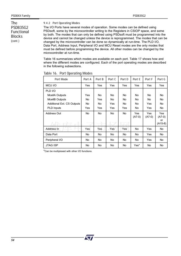
The
PSD835G2
Functional
Blocks
(cont.)
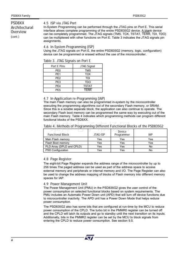
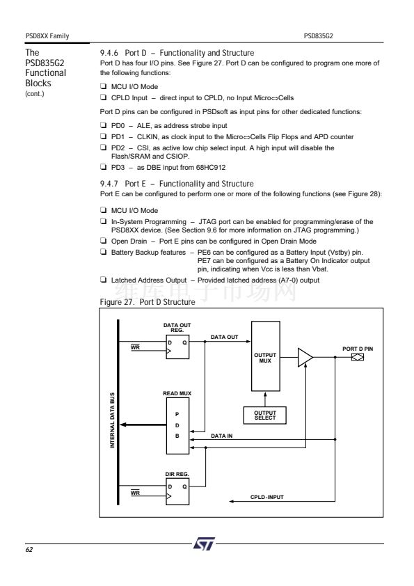
9.4.6 Port D 鈥?Functionality and Structure
Port D has four I/O pins. See Figure 27. Port D can be configured to program one more of
the following functions:
t
MCU I/O Mode
t
CPLD Input 鈥?direct input to CPLD, no Input Micro鈬擟ells
Port D pins can be configured in PSDsoft as input pins for other dedicated functions:
t
PD0 鈥?ALE, as address strobe input
t
PD1 鈥?CLKIN, as clock input to the Micro鈬擟ells Flip Flops and APD counter
t
PD2 鈥?CSI, as active low chip select input. A high input will disable the
Flash/SRAM and CSIOP.
t
PD3 鈥?as DBE input from 68HC912
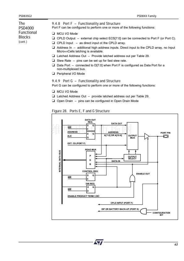
9.4.7 Port E 鈥?Functionality and Structure
Port E can be configured to perform one or more of the following functions (see Figure 28):
t
MCU I/O Mode
t
In-System Programming 鈥?JTAG port can be enabled for programming/erase of the
PSD8XX device. (See Section 9.6 for more information on JTAG programming.)
t
Open Drain 鈥?Port E pins can be configured in Open Drain Mode
t
Battery Backup features 鈥?PE6 can be configured as a Battery Input (Vstby) pin.
PE7 can be configured as a Battery On Indicator output
pin, indicating when Vcc is less than Vbat.
t
Latched Address Output 鈥?Provided latched address (A7-0) output
Figure 27. Port D Structure
DATA OUT
REG.
DATA OUT
D
WR
OUTPUT
MUX
Q
PORT D PIN
INTERNAL DATA BUS
READ MUX
P
D
B
DATA IN
OUTPUT
SELECT
DIR REG.
D
WR
Q
CPLD - INPUT
62


 1
1
 2
2
 3
3
 4
4
 5
5
 6
6
 7
7
 8
8
 9
9
 10
10
 11
11
 12
12
 13
13
 14
14
 15
15
 16
16
 17
17
 18
18
 19
19
 20
20
 21
21
 22
22
 23
23
 24
24
 25
25
 26
26
 27
27
 28
28
 29
29
 30
30
 31
31
 32
32
 33
33
 34
34
 35
35
 36
36
 37
37
 38
38
 39
39
 40
40
 41
41
 42
42
 43
43
 44
44
 45
45
 46
46
 47
47
 48
48
 49
49
 50
50
 51
51
 52
52
 53
53
 54
54
 55
55
 56
56
 57
57
 58
58
 59
59
 60
60
 61
61
 62
62
 63
63
 64
64
 65
65
 66
66
 67
67
 68
68
 69
69
 70
70
 71
71
 72
72
 73
73
 74
74
 75
75
 76
76
 77
77
 78
78
 79
79
 80
80
 81
81
 82
82
 83
83
 84
84
 85
85
 86
86
 87
87
 88
88
 89
89
 90
90
 91
91
 92
92
 93
93
 94
94
 95
95
 96
96
 97
97
 98
98
 99
99
 100
100
 101
101
 102
102
 103
103
 104
104
 105
105
 106
106
 107
107
 108
108
 109
109
 110
110
