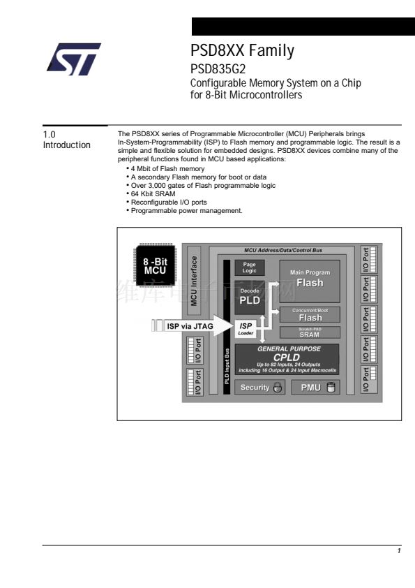
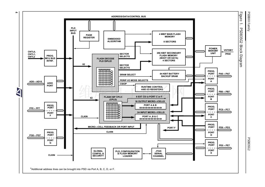
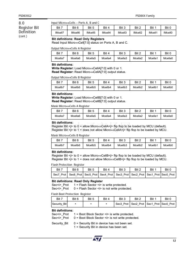
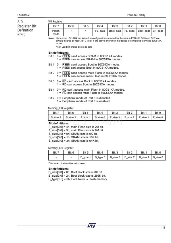
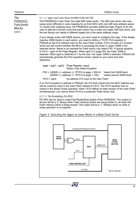
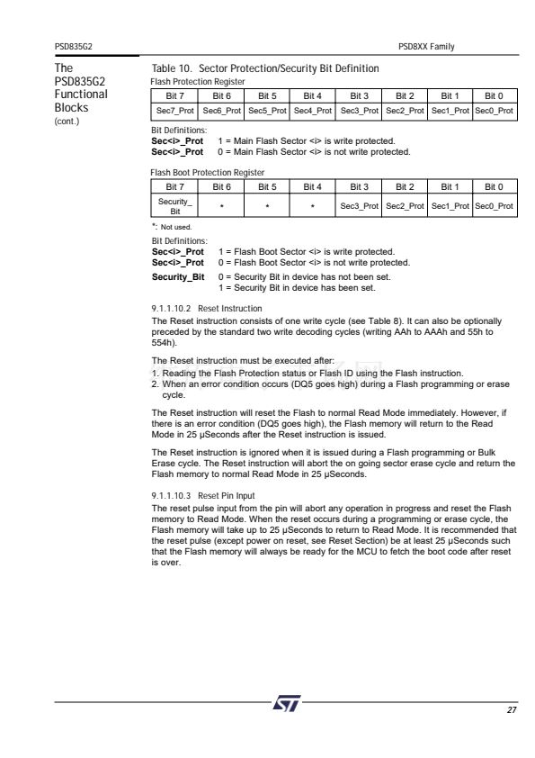
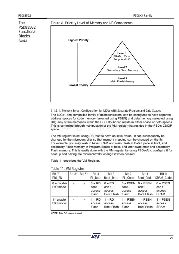
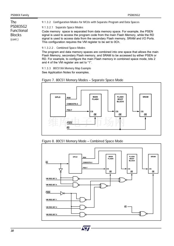
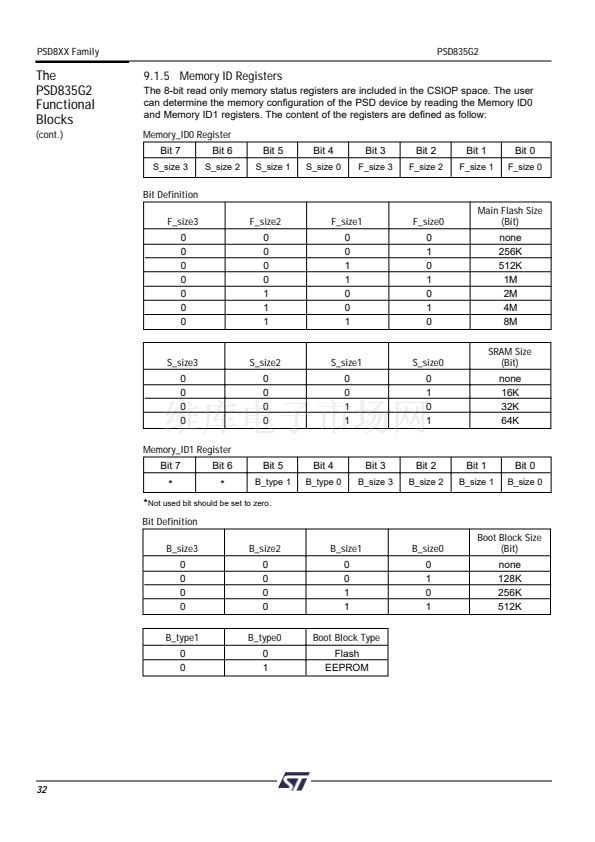
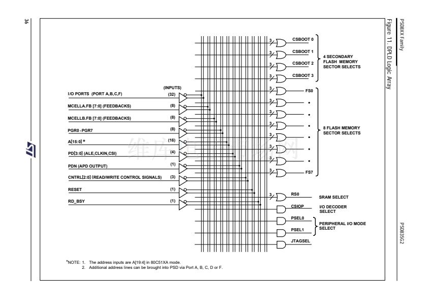
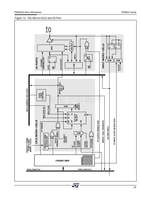
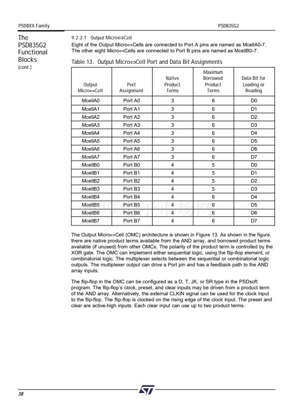
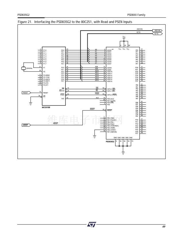
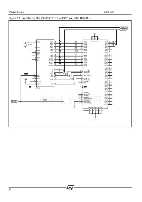
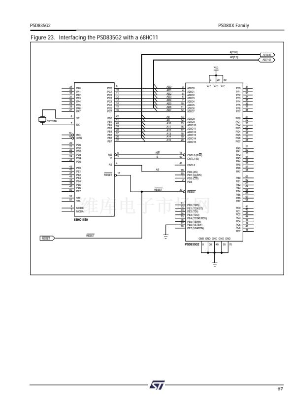
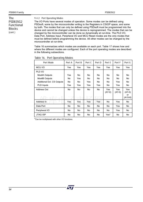
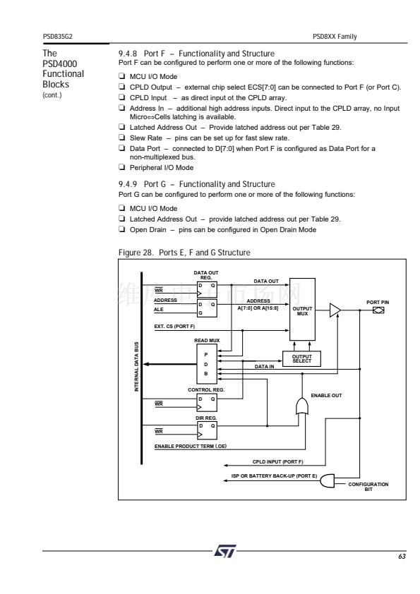
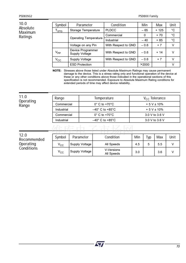
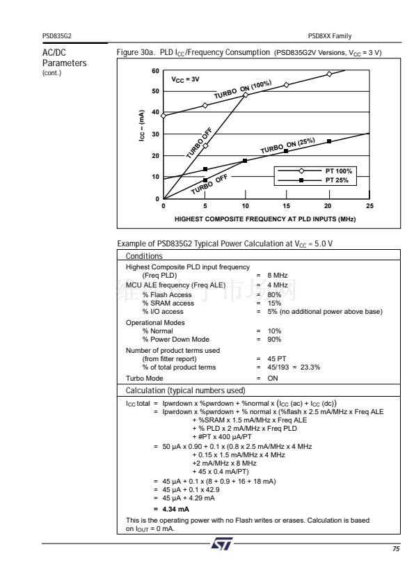
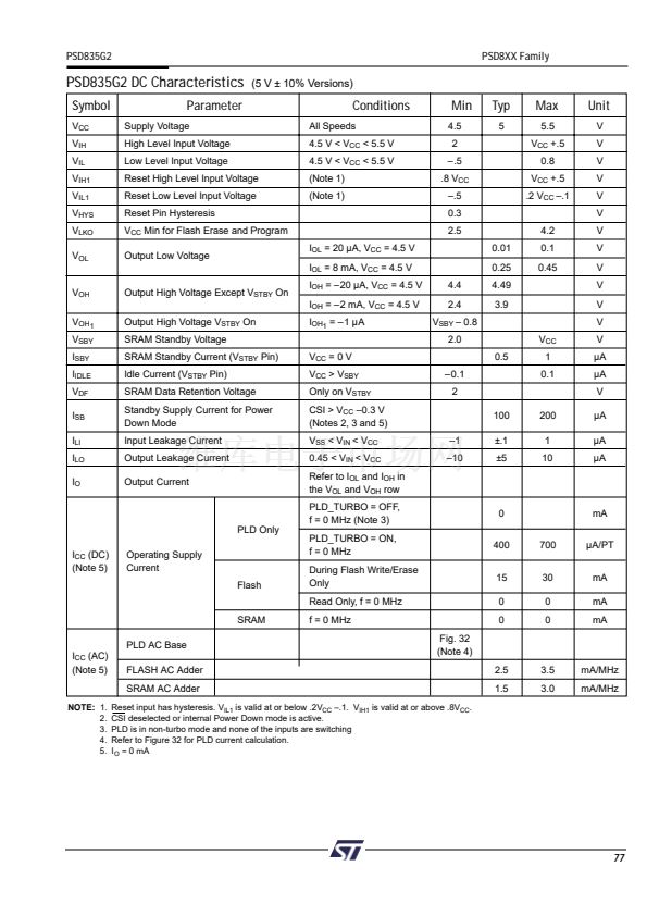
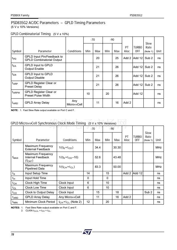
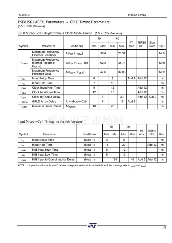
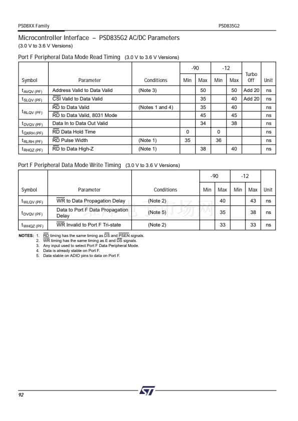
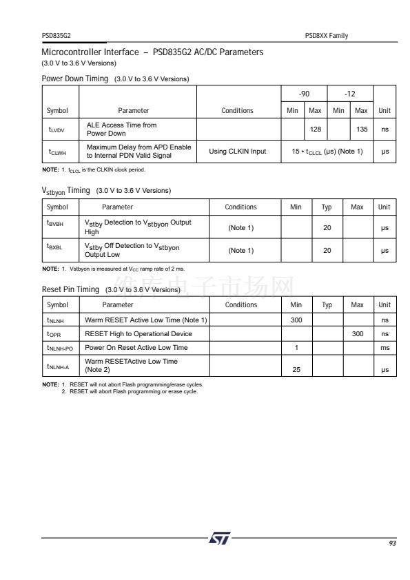
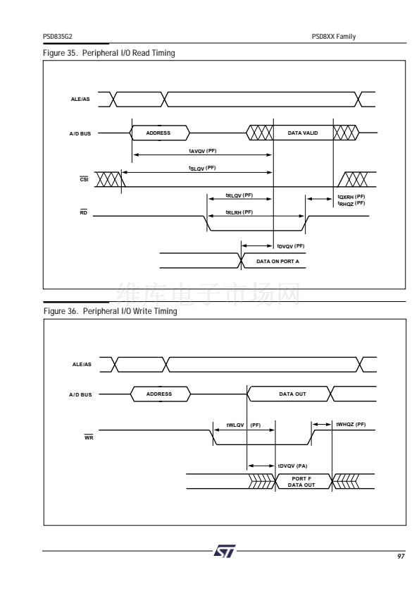
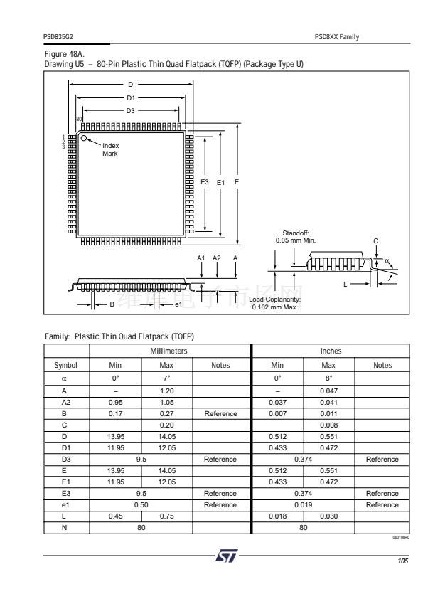
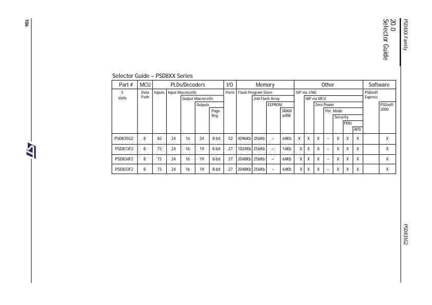
PSD8XX Family
PSD835G2
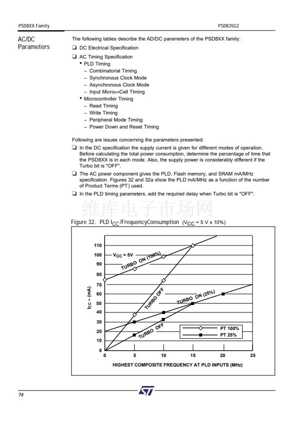
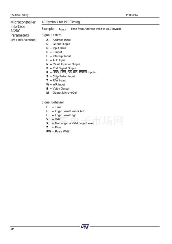
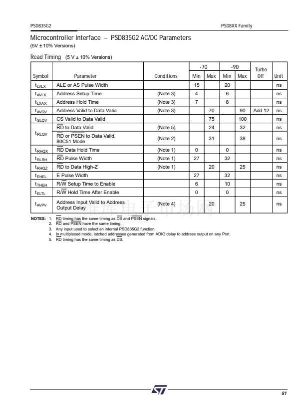
Microcontroller Interface 鈥?PSD835G2 AC/DC Parameters
(5V 卤 10% Versions)
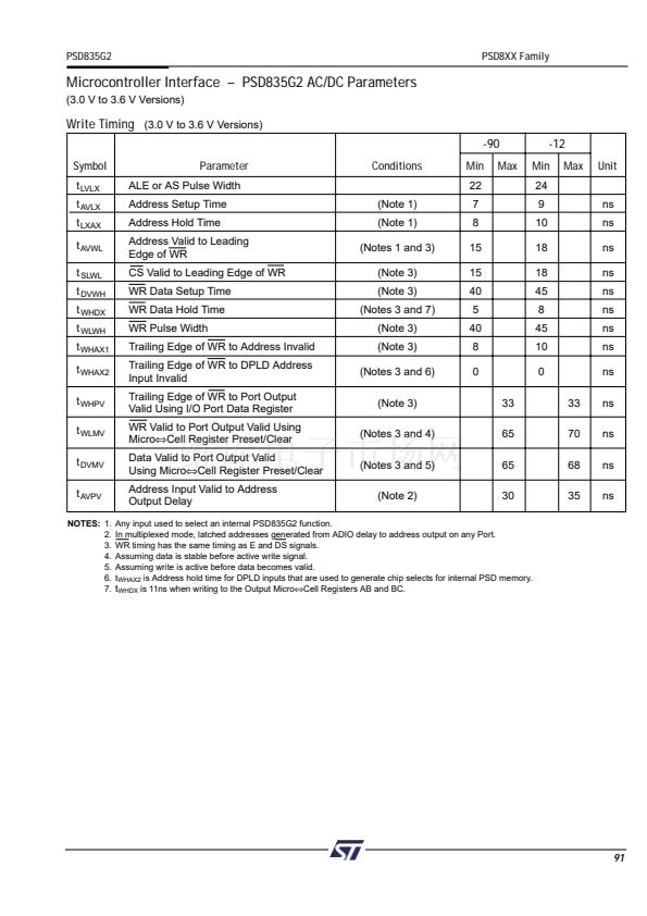
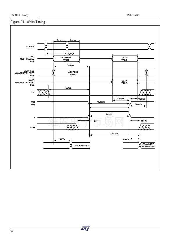
Write Timing
(5 V 卤 10% Versions)
-70
Symbol
t
LVLX
t
AVLX
t
LXAX
t
AVWL
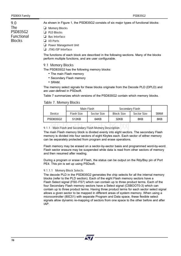
t
SLWL
t
DVWH
t
WHDX
t
WLWH
t
WHAX1
t
WHAX2
t
WHPV
t
WLMV
t
DVMV
t
AVPV
NOTES:
1.
2.
3.
4.
5.
6.
7.
-90
Min
20
6
8
15
15
35
5
35
8
0
27
48
42
30
55
55
ns
ns
ns
ns
ns
ns
ns
ns
ns
ns
ns
ns
Parameter
ALE or AS Pulse Width
Address Setup Time
Address Hold Time
Address Valid to Leading
Edge of WR
CS Valid to Leading Edge of WR
WR Data Setup Time
WR Data Hold Time
WR Pulse Width
Trailing Edge of WR to Address
Invalid
Trailing Edge of WR to DPLD
Address Input Invalid
Trailing Edge of WR to Port Output
Valid Using I/O Port Data Register
WR Valid to Port Output Valid Using
Micro鈬擟ell Register Preset/Clear
Data Valid to Port Output Valid
Using Micro鈬擟ell Register
Preset/Clear
Address Input Valid to Address
Output Delay
Conditions
(Note 1)
(Note 1)
(Notes 1 and 3)
(Note 3)
(Note 3)
(Notes 3 and 7)
(Note 3)
(Note 3)
(Note 3 and 6)
(Note 3)
(Notes 3 and 4)
(Notes 3 and 5)
Min
15
4
7
8
12
25
4
28
6
0
Max
Max
Unit
(Note 2)
20
25
ns
Any input used to select an internal PSD8XX function.
In multiplexed mode, latched addresses generated from ADIO delay to address output on any Port.
WR timing has the same timing as E and DS signals.
Assuming data is stable before active write signal.
Assuming write is active before data becomes valid.
t
WHAX2
is Address Hold Time for DPLD inputs that are used to generate chip selects for internal PSD memory.
t
WHDX
is 6ns when writing to the Output Micro鈬擟ell Registers AB and BC.
82


 1
1
 2
2
 3
3
 4
4
 5
5
 6
6
 7
7
 8
8
 9
9
 10
10
 11
11
 12
12
 13
13
 14
14
 15
15
 16
16
 17
17
 18
18
 19
19
 20
20
 21
21
 22
22
 23
23
 24
24
 25
25
 26
26
 27
27
 28
28
 29
29
 30
30
 31
31
 32
32
 33
33
 34
34
 35
35
 36
36
 37
37
 38
38
 39
39
 40
40
 41
41
 42
42
 43
43
 44
44
 45
45
 46
46
 47
47
 48
48
 49
49
 50
50
 51
51
 52
52
 53
53
 54
54
 55
55
 56
56
 57
57
 58
58
 59
59
 60
60
 61
61
 62
62
 63
63
 64
64
 65
65
 66
66
 67
67
 68
68
 69
69
 70
70
 71
71
 72
72
 73
73
 74
74
 75
75
 76
76
 77
77
 78
78
 79
79
 80
80
 81
81
 82
82
 83
83
 84
84
 85
85
 86
86
 87
87
 88
88
 89
89
 90
90
 91
91
 92
92
 93
93
 94
94
 95
95
 96
96
 97
97
 98
98
 99
99
 100
100
 101
101
 102
102
 103
103
 104
104
 105
105
 106
106
 107
107
 108
108
 109
109
 110
110
