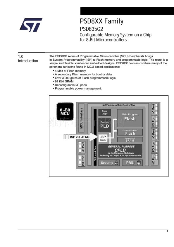
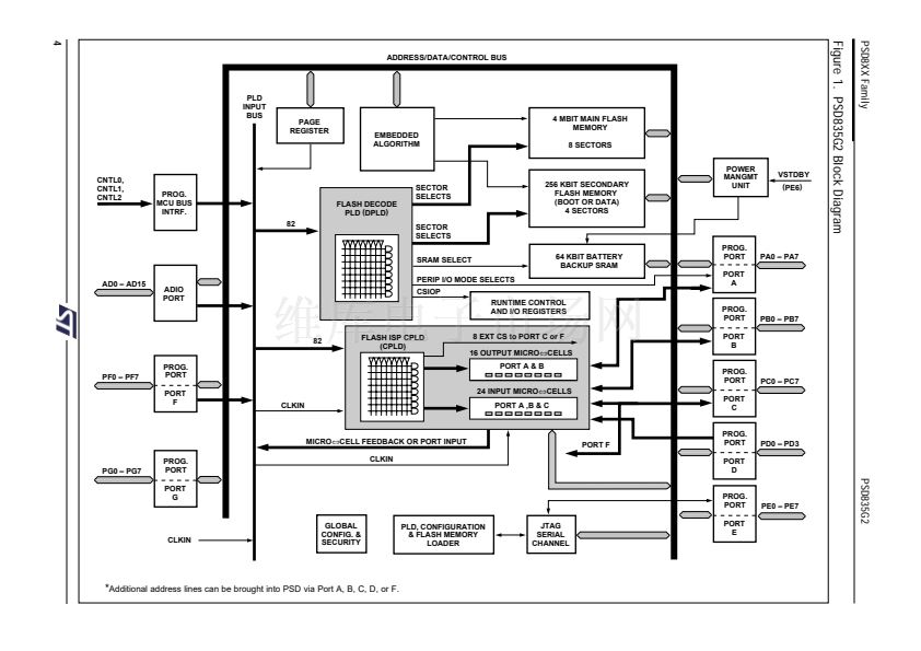
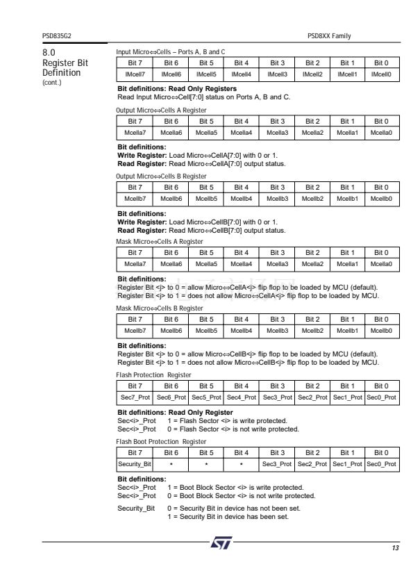
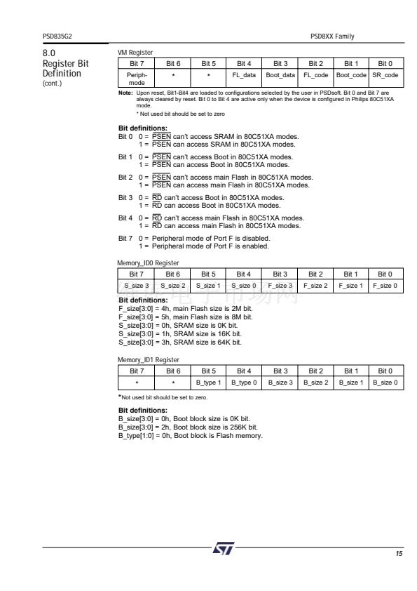
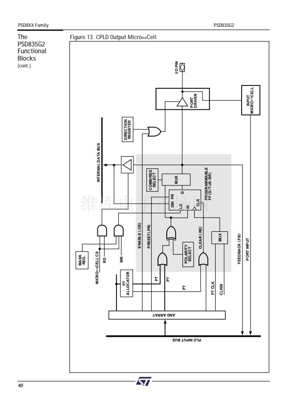
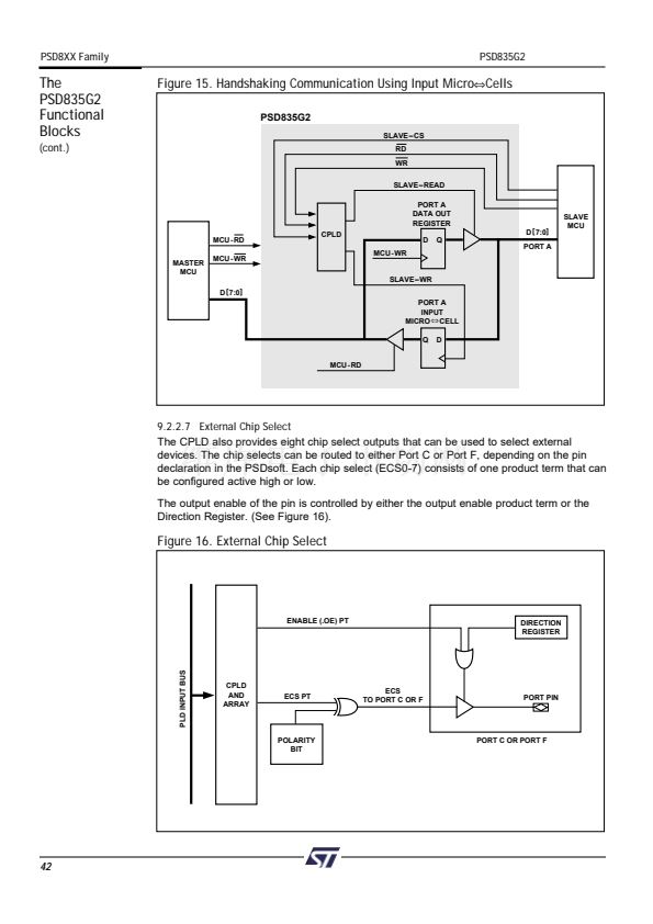
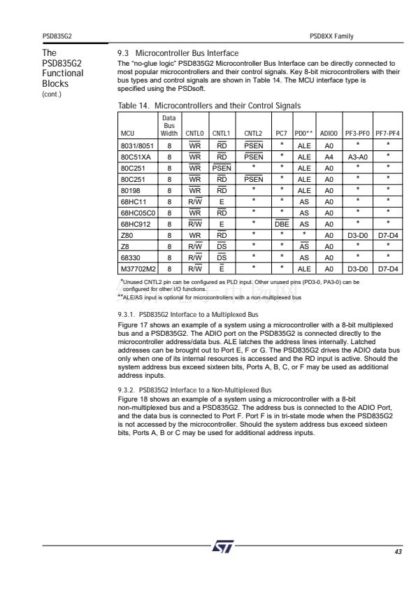
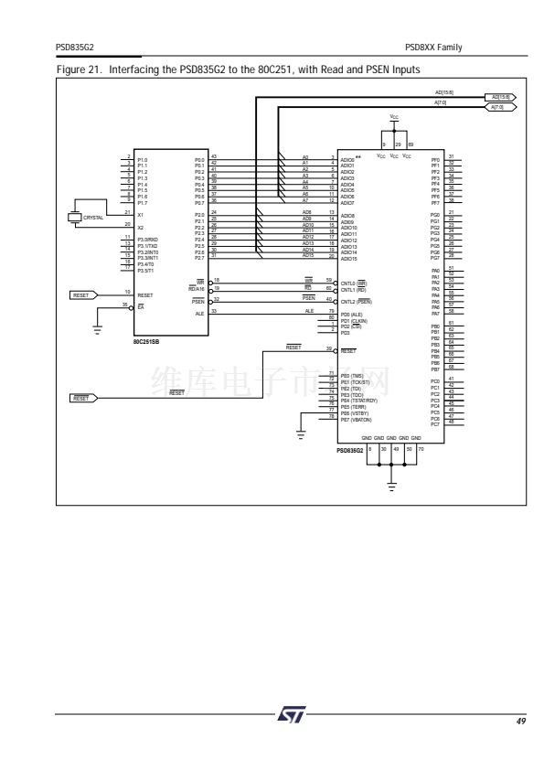
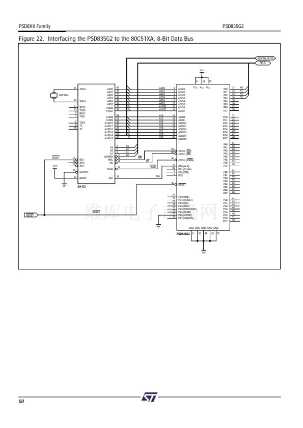
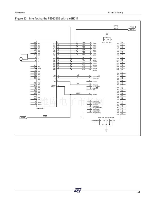
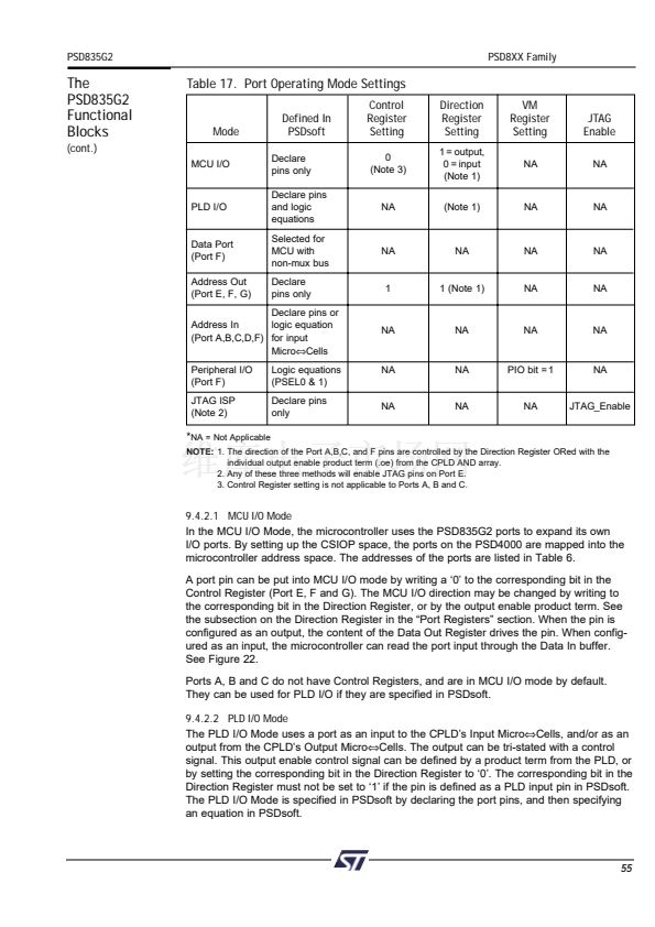
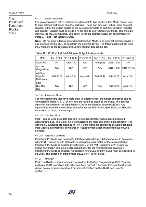
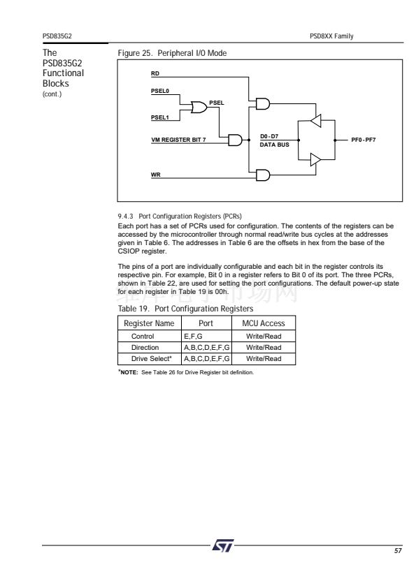
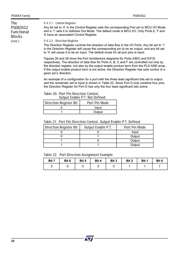
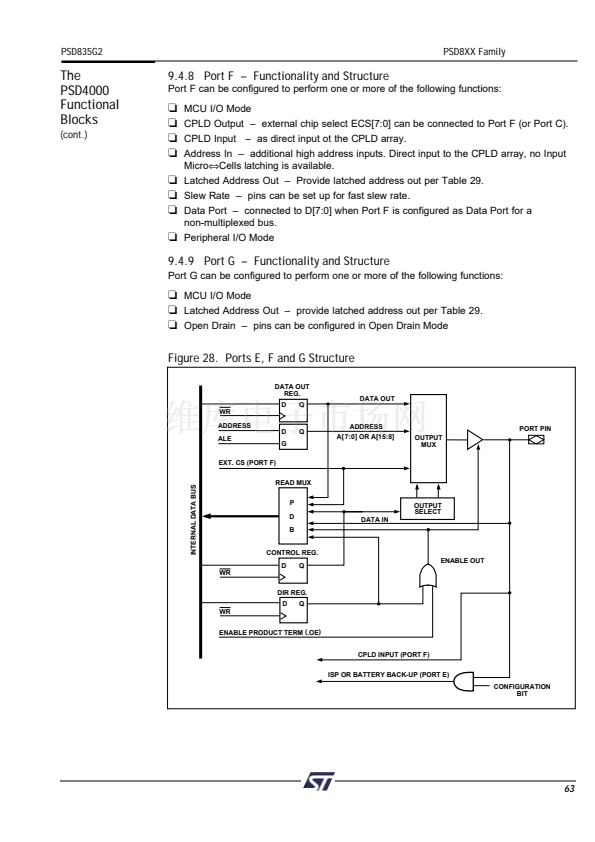
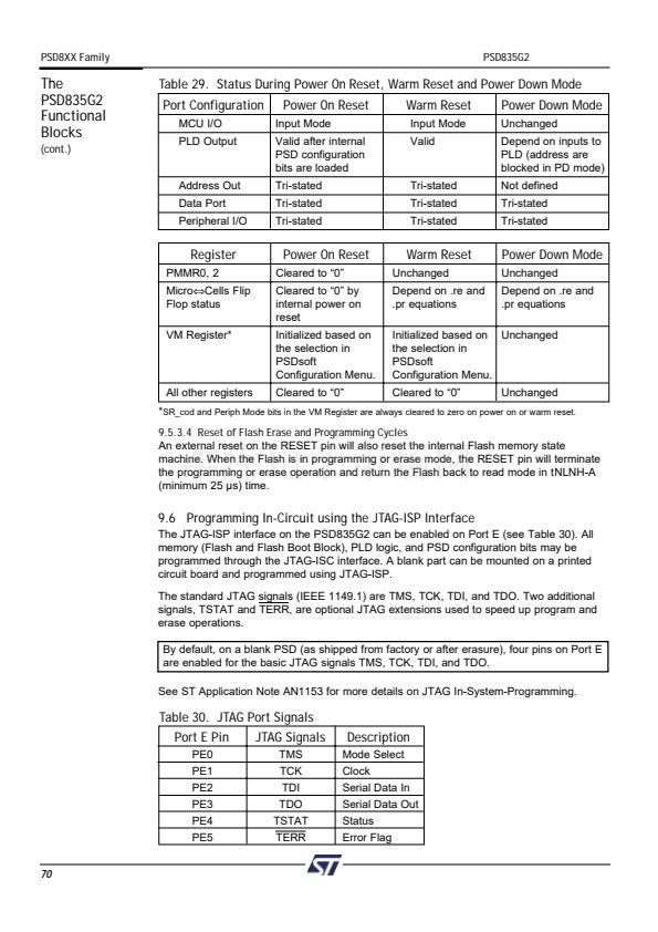
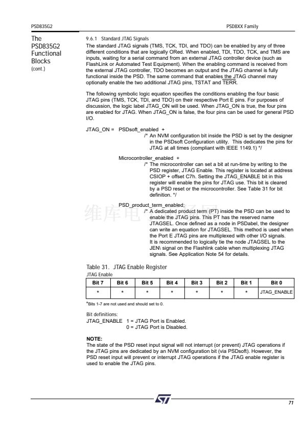
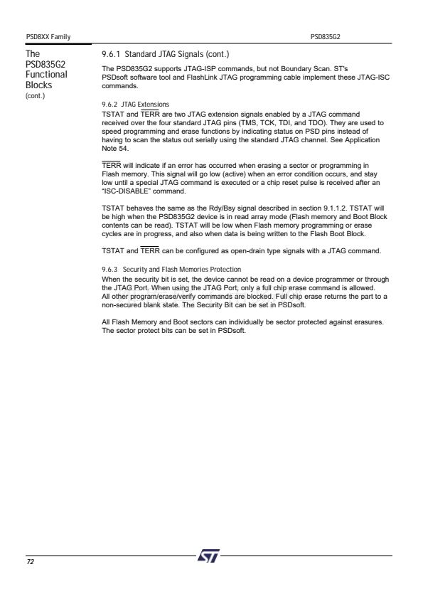
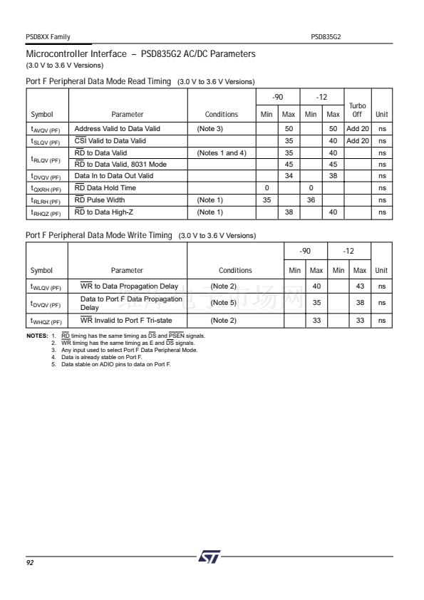
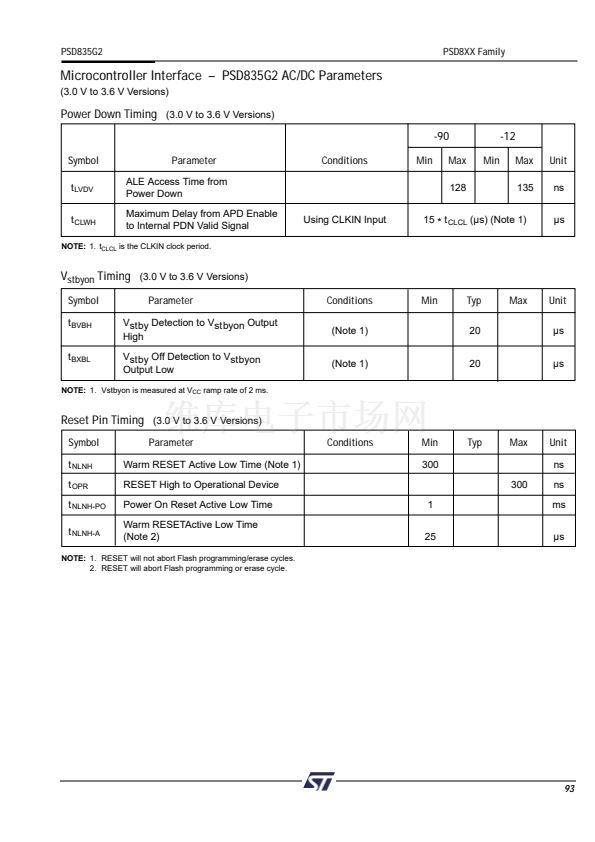
PSD8XX Family
PSD835G2
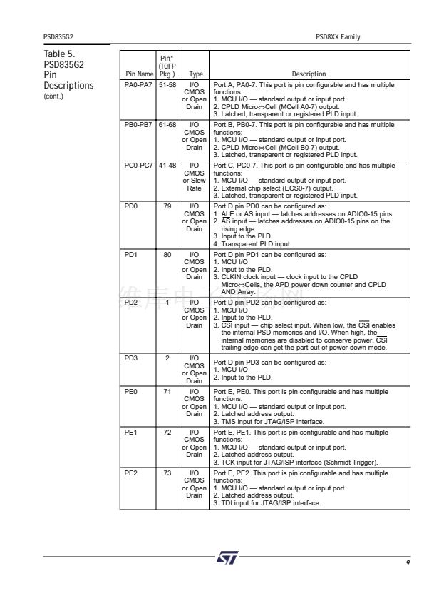
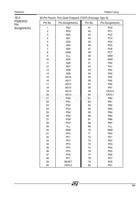
The following table describes the pin names and pin functions of the PSD835G2. Pins that
have multiple names and/or functions are defined using PSDsoft.
Pin*
(TQFP
Pkg.)
3-7
10-12
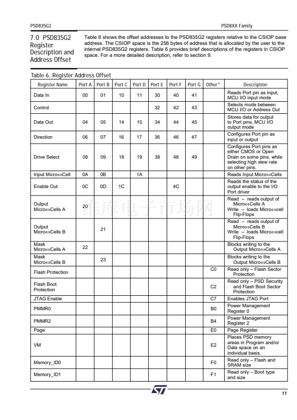
6.0
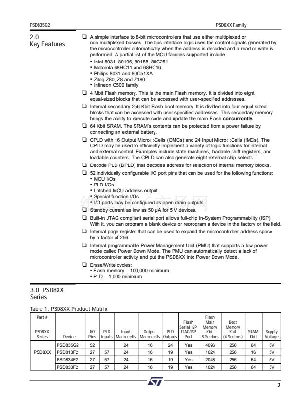
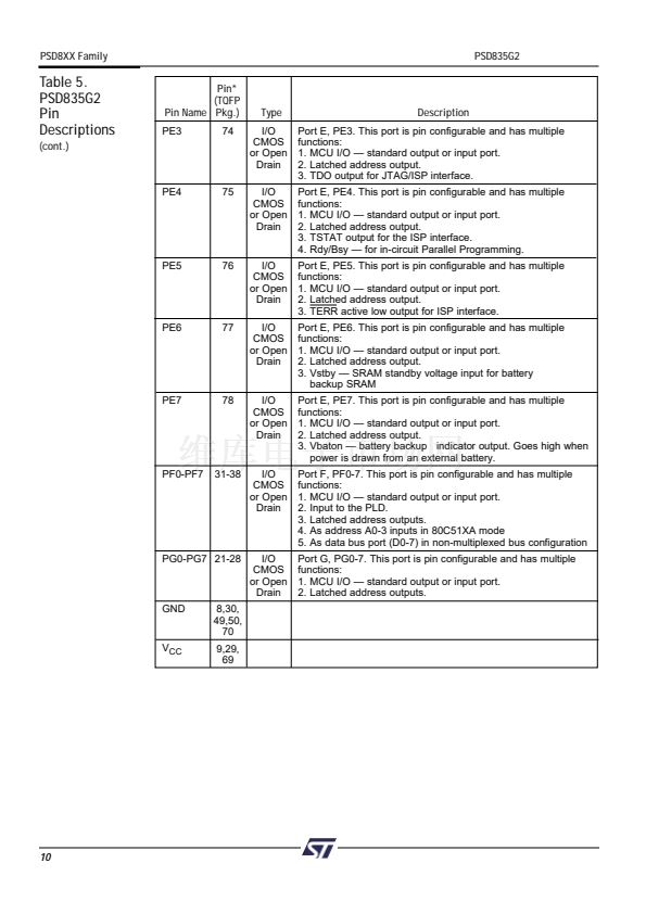
Table 5.
PSD835G2
Pin
Descriptions
Pin Name
ADIO0-7
Type
I/O
Description
This is the lower Address/Data port. Connect your MCU
address or address/data bus according to the following rules:
1. If your MCU has a multiplexed address/data bus where the
data is multiplexed with the lower address bits, connect
AD[0:7] to this port.
2. If your MCU does not have a multiplexed address/data bus,
connect A[0:7] to this port.
3. If you are using an 80C51XA in burst mode, connect
A4/D0 through A11/D7 to this port.
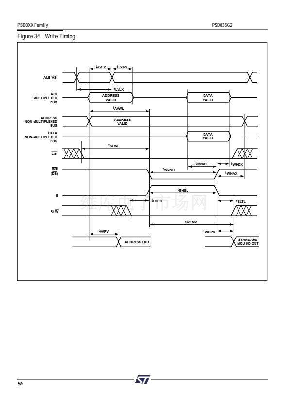
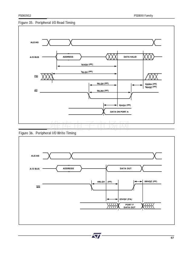
ALE or AS latches the address. The PSD drives data out only
if the read signal is active and one of the PSD functional blocks
was selected. The addresses on this port are passed to the
PLDs.
This is the upper Address/Data port. Connect your MCU
address or address/data bus according to the following rules:
1. If your MCU has a multiplexed address/data bus where the
data is multiplexed with the lower address bits, connect
A[8:15] to this port.
2. If your MCU does not have a multiplexed address/data bus,
connect A[8:15] to this port.
3. If you are using an 80C251 in page mode, connect AD[8:15]
to this port
4. If you are using an 80C51XA in burst mode, connect
A[12:19] to this port.
ALE or AS latches the address. The PSD drives data out only
if the read signal is active and one of the PSD functional
blocks was selected. The addresses on this port are passed
to the PLDs.
The following control signals can be connected to this port,
based on your MCU:
1. WR 鈥?active-low write input.
2. R_W 鈥?active-high read/active low write input.
This pin is connected to the PLDs. Therefore, these signals can
be used in decode and other logic equations.
The following control signals can be connected to this port,
based on your MCU:
1. RD 鈥?active-low read input.
2. E 鈥?E clock input.
3. DS 鈥?active-low data strobe input.
4. PSEN 鈥?connect PSEN to this port when it is being used as
an active-low read signal. For example, when the 80C251
outputs more than 16 address bits, PSEN is actually the read
signal.
This pin is connected to the PLDs. Therefore, these signals can
be used in decode and other logic equations.
This pin can be used to input the PSEN (Program Select
Enable) signal from any MCU that uses this signal for code
exclusively. If your MCU does not output a Program Select
Enable signal, this port can be used as a generic input. This
port is connected to the PLD as input.
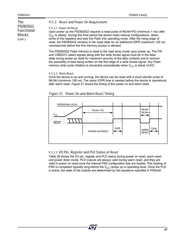
Active low input. Resets I/O Ports, PLD Micro鈬擟ells, some of
the configuration registers and JTAG registers. Must be active
at power up. Reset also aborts the Flash programming/erase
cycle that is in progress.
ADIO8-15
13-20
I/O
CNTL0
59
I
CNTL1
60
I
CNTL2
40
I
Reset
39
I
8


 1
1
 2
2
 3
3
 4
4
 5
5
 6
6
 7
7
 8
8
 9
9
 10
10
 11
11
 12
12
 13
13
 14
14
 15
15
 16
16
 17
17
 18
18
 19
19
 20
20
 21
21
 22
22
 23
23
 24
24
 25
25
 26
26
 27
27
 28
28
 29
29
 30
30
 31
31
 32
32
 33
33
 34
34
 35
35
 36
36
 37
37
 38
38
 39
39
 40
40
 41
41
 42
42
 43
43
 44
44
 45
45
 46
46
 47
47
 48
48
 49
49
 50
50
 51
51
 52
52
 53
53
 54
54
 55
55
 56
56
 57
57
 58
58
 59
59
 60
60
 61
61
 62
62
 63
63
 64
64
 65
65
 66
66
 67
67
 68
68
 69
69
 70
70
 71
71
 72
72
 73
73
 74
74
 75
75
 76
76
 77
77
 78
78
 79
79
 80
80
 81
81
 82
82
 83
83
 84
84
 85
85
 86
86
 87
87
 88
88
 89
89
 90
90
 91
91
 92
92
 93
93
 94
94
 95
95
 96
96
 97
97
 98
98
 99
99
 100
100
 101
101
 102
102
 103
103
 104
104
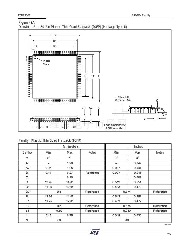
 105
105
 106
106
 107
107
 108
108
 109
109
 110
110
