PSD8XX Family
PSD835G2
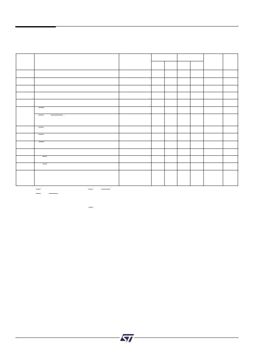
Microcontroller Interface 鈥?PSD835G2 AC/DC Parameters
(3.0 V to 3.6 V Versions)
Read Timing
(3.0 V to 3.6 V Versions)
-90
Symbol
t
LVLX
t
AVLX
t
LXAX
t
AVQV
t
SLQV
t
RLQV
t
RHQX
t
RLRH
t
RHQZ
t
EHEL
t
THEH
t
ELTL
t
AVPV
NOTES:
1.
2.
3.
4.
5.
-12
Min
24
9
10
90
90
35
45
Parameter
ALE or AS Pulse Width
Address Setup Time
Address Hold Time
Address Valid to Data Valid
CS Valid to Data Valid
RD to Data Valid
RD or PSEN to Data Valid,
80C51XA Mode
RD Data Hold Time
RD Pulse Width
RD to Data High-Z
E Pulse Width
R/W Setup Time to Enable
R/W Hold Time After Enable
Address Input Valid to
Address Output Delay
Conditions
(Note 3)
(Note 3)
(Note 3)
(Note 5)
(Note 2)
(Note 1)
(Note 1)
(Note 1)
Min
22
7
8
Max
Max
Turbo
Off
Unit
ns
ns
ns
120 Add 20**
120
35
48
0
40
ns
ns
ns
ns
ns
ns
0
36
38
38
10
0
40
42
16
0
ns
ns
ns
ns
(Note 4)
30
35
ns
RD timing has the same timing as DS and PSEN signals.
RD and PSEN have the same timing for 80C51.
Any input used to select an internal PSD835G2V function.
In multiplexed mode latched address generated from ADIO delay to address output on any Port.
RD timing has the same timing as DS.
90
