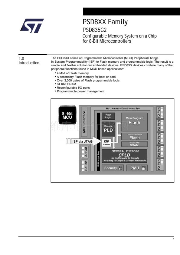
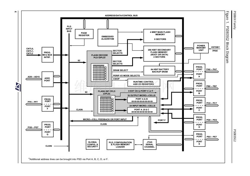
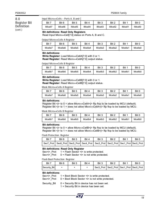
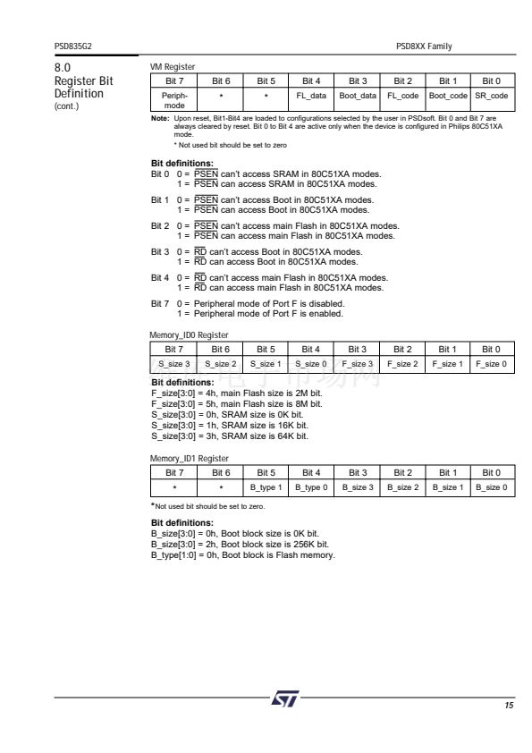
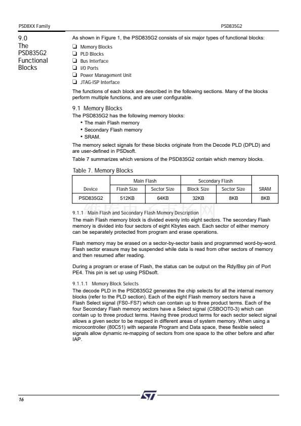
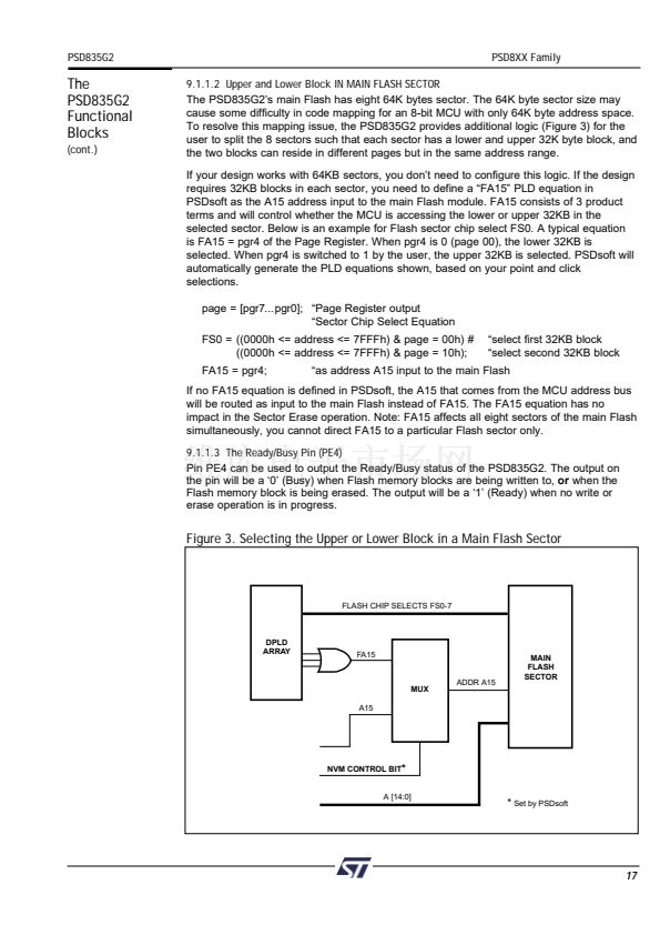
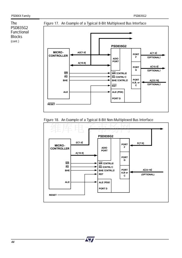
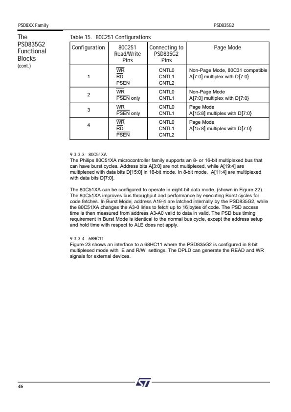
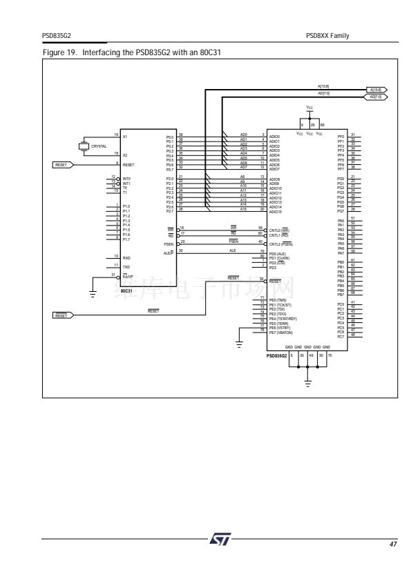
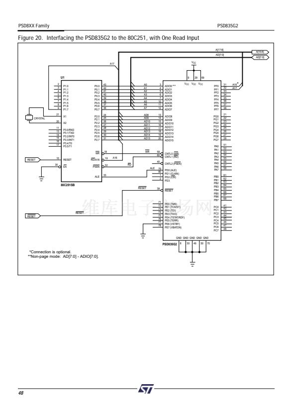
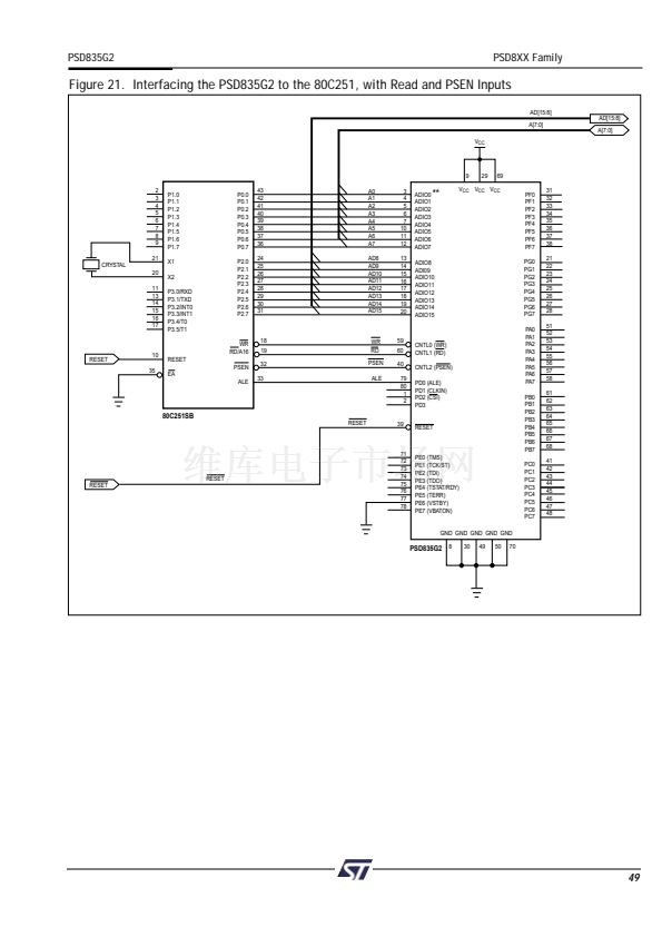
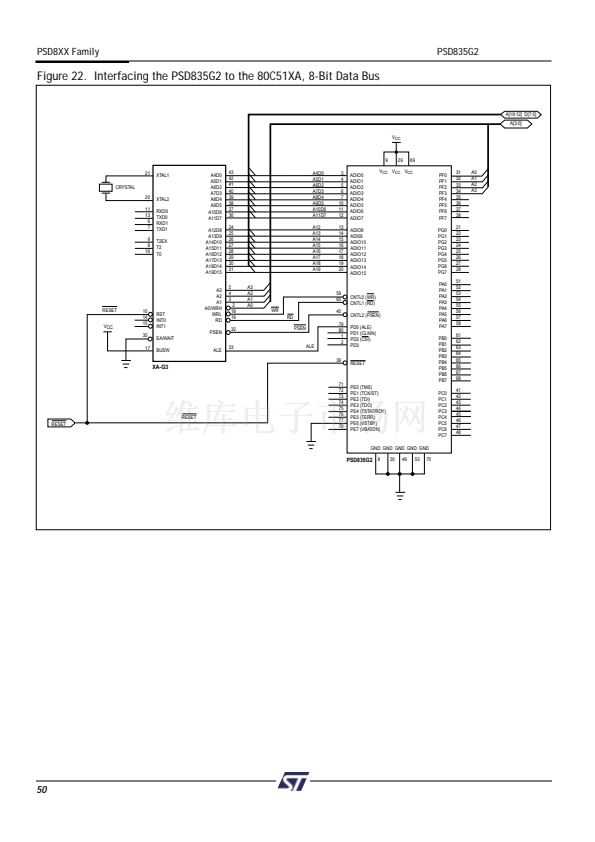
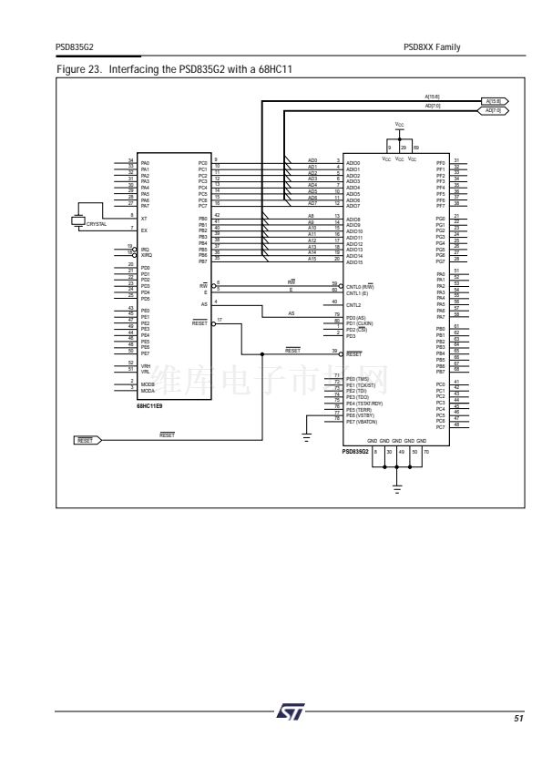
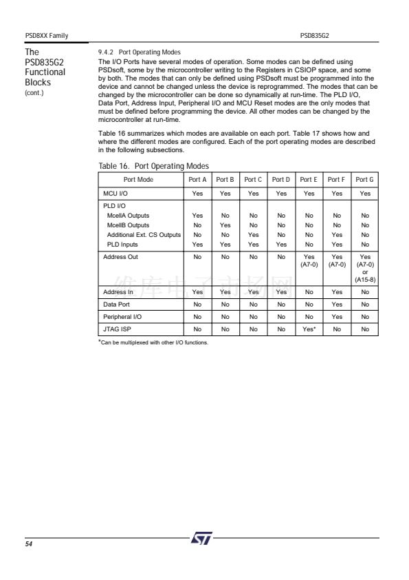
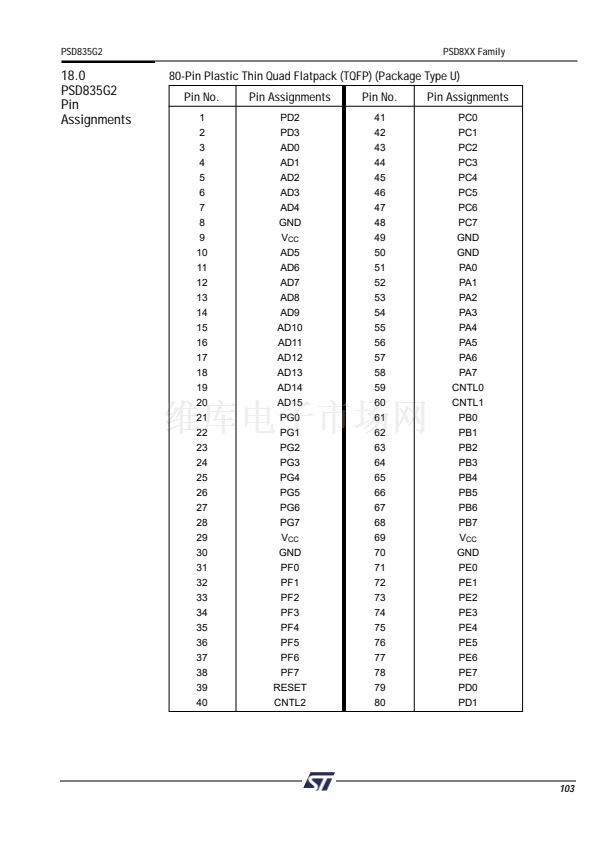
PSD835G2
PSD8XX Family
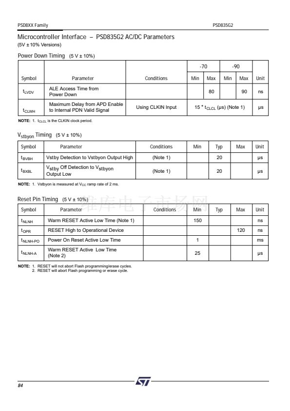
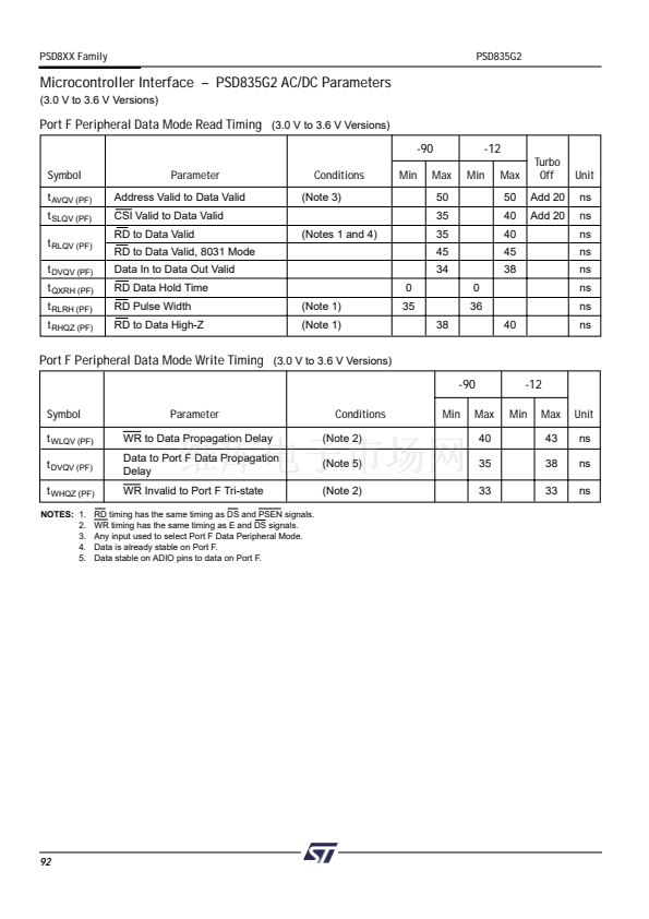
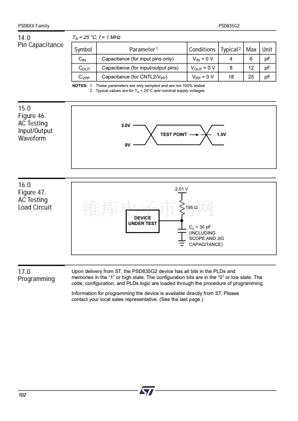
Microcontroller Interface 鈥?PSD835G2 AC/DC Parameters
(3.0 V to 3.6 V Versions)
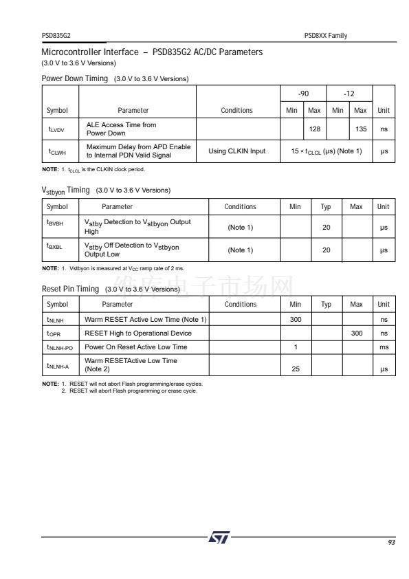
Power Down Timing
(3.0 V to 3.6 V Versions)
-90
Symbol
t
LVDV
t
CLWH
-12
Min
Max
135
Parameter
ALE Access Time from
Power Down
Maximum Delay from APD Enable
to Internal PDN Valid Signal
Conditions
Min
Max
128
Unit
ns
碌s
Using CLKIN Input
15
*
t
CLCL
(碌s) (Note 1)
NOTE:
1. t
CLCL
is the CLKIN clock period.
V
stbyon
Timing
(3.0 V to 3.6 V Versions)
Symbol
t
BVBH
t
BXBL
Parameter
Vstby Detection to Vstbyon Output
High
Vstby Off Detection to Vstbyon
Output Low
Conditions
(Note 1)
(Note 1)
Min
Typ
20
20
Max
Unit
碌s
碌s
NOTE:
1. Vstbyon is measured at V
CC
ramp rate of 2 ms.
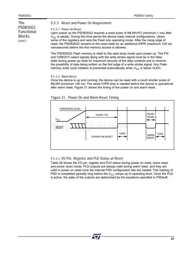
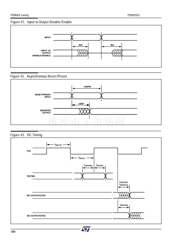
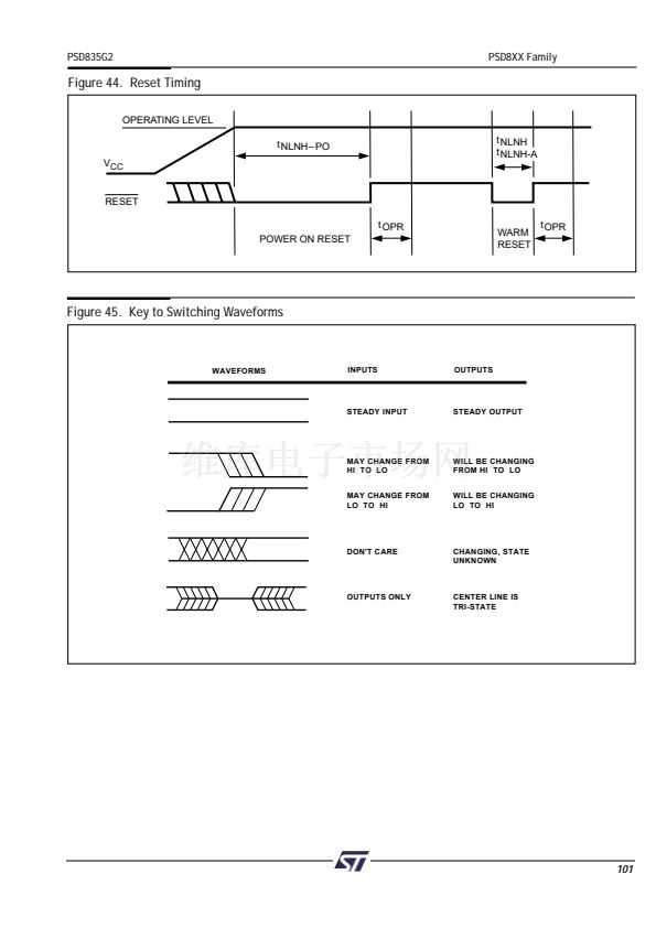
Reset Pin Timing
(3.0 V to 3.6 V Versions)
Symbol
t
NLNH
t
OPR
t
NLNH-PO
t
NLNH-A
Parameter
Warm RESET Active Low Time (Note 1)
RESET High to Operational Device
Power On Reset Active Low Time
Warm RESETActive Low Time
(Note 2)
Conditions
Min
300
Typ
Max
Unit
ns
300
1
25
ns
ms
碌s
NOTE:
1. RESET will not abort Flash programming/erase cycles.
2. RESET will abort Flash programming or erase cycle.
93


 1
1
 2
2
 3
3
 4
4
 5
5
 6
6
 7
7
 8
8
 9
9
 10
10
 11
11
 12
12
 13
13
 14
14
 15
15
 16
16
 17
17
 18
18
 19
19
 20
20
 21
21
 22
22
 23
23
 24
24
 25
25
 26
26
 27
27
 28
28
 29
29
 30
30
 31
31
 32
32
 33
33
 34
34
 35
35
 36
36
 37
37
 38
38
 39
39
 40
40
 41
41
 42
42
 43
43
 44
44
 45
45
 46
46
 47
47
 48
48
 49
49
 50
50
 51
51
 52
52
 53
53
 54
54
 55
55
 56
56
 57
57
 58
58
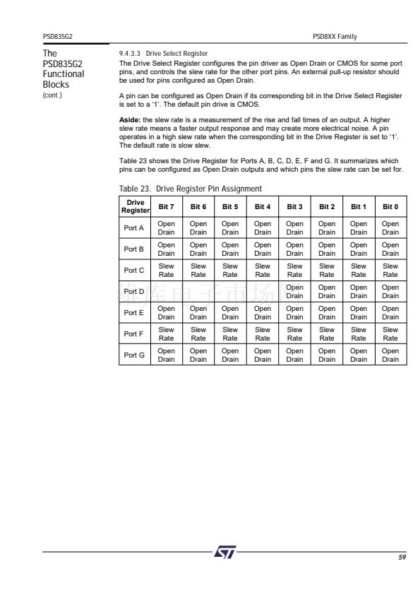
 59
59
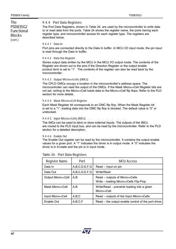
 60
60
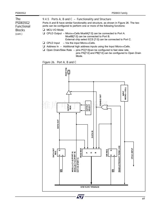
 61
61
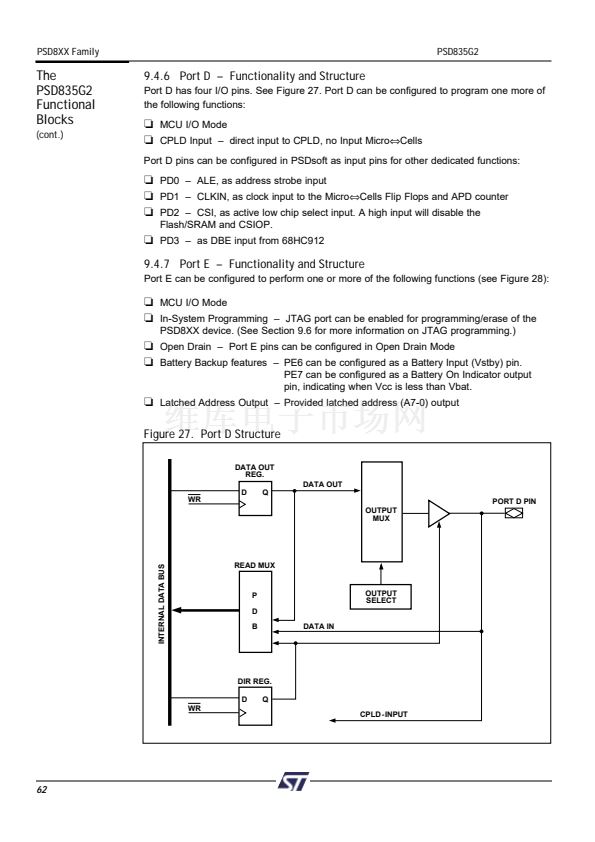
 62
62
 63
63
 64
64
 65
65
 66
66
 67
67
 68
68
 69
69
 70
70
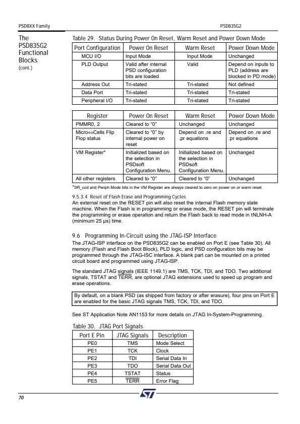 71
71
 72
72
 73
73
 74
74
 75
75
 76
76
 77
77
 78
78
 79
79
 80
80
 81
81
 82
82
 83
83
 84
84
 85
85
 86
86
 87
87
 88
88
 89
89
 90
90
 91
91
 92
92
 93
93
 94
94
 95
95
 96
96
 97
97
 98
98
 99
99
 100
100
 101
101
 102
102
 103
103
 104
104
 105
105
 106
106
 107
107
 108
108
 109
109
 110
110
